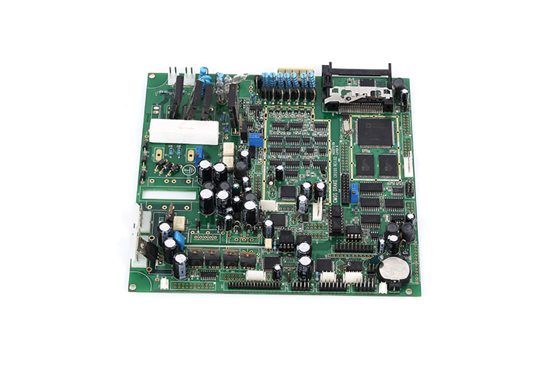
What Is Via in Pad
Via in Pad is a technology commonly used in PCB design, which allows the pins of electronic components to be directly connected to the vias located in pad. It provides a more compact and reliable connection method.
The Main Advantages of The Via in Pad Process Are As Follows:
1) Reduce the number of pads: The number of component pins can be reduced by embedding via holes in pads, thereby providing greater layout space. This is particularly important for high-density and small-sized PCB designs.
2) Improve signal integrity: Reduce pin length and circuit paths by connecting the pins directly to the via holes in pads, resulting in reduced signal delay and interference. This helps improve signal integrity and circuit performance.
3) Improve thermal management: The Via in Pad process can also be used for thermal management. Heat can be conducted and dispersed more effectively by placing a thermal pad or heat sink in the pad.
4) Improve reliability: Hole-in-pad process can provide more reliable pin connection. The mechanical stress and strain on the pins is reduced by connecting the pins directly to the pads, thereby reducing the risk of pins breakage or detachment.
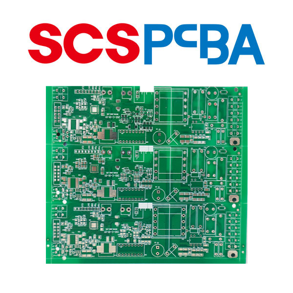
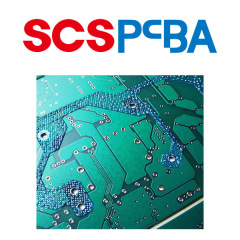
The via-in-pad technology increases manufacturing costs because it requires more complex manufacturing process and specialized production equipment. SCSPCBA is a professional manufacturer for Via-in-Pad PCB, our professional team can provide you with the perfect solutions. About the cost and technical details, please feel free to contact us.