HOME /Products /PCBA Services /PCBA Design Scheme
☑ Circuit Layout Design
☑ Quote Instantly Online!
☑ ISO9001 & UL Certified
☑ Complete PCBA Solutions
PCBA Design Scheme
SCSPCBA Usually Uses 3 Types PCBA Design Schemes
· Manual Design
Manual design involves using specialized software to create a schematic for a printed circuit board and using the schematic to create a layout for the board.
The advantage is: it provides more flexibility and control over the PCBA design process
The downside: this method is time-consuming and requires a high level of expertise
· Automation Design
The automated design uses computer-aided design (CAD) software to create the PCB layout.
Advantages: Automated design can design faster and more accurately, saving time
Cons: It's not as flexible as manual design. The automated design also requires specialized software and expertise.
· Hybrid Design
Hybrid designs combine manual and automated design methods. SCSPCBA uses automated design software to create the basic layout of the PCB, which is then fine-tuned manually.
This approach combines the best of both worlds and allows for greater flexibility and control over the design process, while also reducing the time required for manual design.
In the actual process, SCSPCBA is based on customer needs, and the choice of PCBA design method depends on the specific needs and requirements of the project, as well as the professional knowledge and resources of our designers.
PCBA (Printed Circuit Board Assembly) design is a complex process that involves several steps.
Scspcba Start To Design The Scheme After Receiving Customers' Requirements
Circuit Design Requirements And Draw Circuit Schematic Diagrams
Clarify the function of the circuit to be designed, as well as the performance index and interface requirements to be met. Create and draw circuit schematics to clarify circuit structure and signal transmission paths. During the design process of SCSPCBA, wiring rules, signal integrity and noise suppression will be considered, and these requirements will determine the overall structure, device selection and layout of PCBA.
Selection of Electronic Components
According to the requirements of circuit design and circuit schematic diagram, SCSPCBA will select electronic components that meet the requirements, including integrated circuits, sensors, capacitors, inductors, transistors, etc.
PCB Layout Design
According to the schematic design, SCSPCBA will select the corresponding circuit components and place them on the PCB board, and the signal and power connections between the circuit components will ensure the best signal transmission quality and the best EMC performance. Factors such as distance, height, direction, impedance matching, and signal integrity between devices should be considered during layout design. We follow wiring rules and EMC specifications.
Gerber File Generation
Once the PCB layout design is complete, the next step is to generate the Gerber files. These files contain the information needed to manufacture the PCB.
PCB Fabrication and Assembly
After the Gerber file is generated, SCSPCBA will manufacture the PCB board and assemble the components.
During the manufacturing process, we need to choose the appropriate PCB material, process and factory, which includes coating a layer of copper on the PCB, and then etching away the unnecessary copper to create the circuit.
Component placement: After the PCB is manufactured, the components are placed on the board. When assembling components, pay attention to the correct orientation of the components, which is usually done using a placement machine
Soldering: After placing the components, solder the PCB. This involves heating and melting the solder, creating a bond between the component and the PCB.
PCBA Functional Testing and Verification
After the soldering is completed, SCSPCBA conducts PCBA board testing and verification to ensure that the circuit performance and reliability meet the requirements. During the test verification process, suitable test tools and methods need to be adopted, which involves testing the connection and function of the components.
Final Assembly
After testing is complete, the PCB is ready for final assembly. This involves mounting the PCB in its housing and connecting any external components such as power supplies and connectors.
SCSPCBA Has Profession PCBA Design Handbook
A PCBA design handbook is a comprehensive guide that provides information, that includes information on design considerations, component selection, assembly processes, and testing procedures.
Design Considerations
Guide design considerations such as board size and shape, trace widths, and clearance distances. It covers topics such as signal integrity, power distribution, and thermal management.
Component Selection
Guide on selecting components such as resistors, capacitors, and integrated circuits. Topics such as component placement and orientation, and the use of surface mount versus through-hole components.
Assembly Processes
Guide assembly processes such as soldering, component placement, and testing. The use of automated versus manual assembly processes, and the importance of quality control during the assembly process.
Testing Procedures
Guide testing procedures such as electrical testing, functional testing, and environmental testing. The use of test fixtures and the importance of validating the performance of the PCB assembly.
Overall, a PCBA design handbook can be a valuable resource for SCSPCBA designers and engineers who are involved in the design, development, and testing of printed circuit board assemblies.
Common Problems in PCBA Design Scheme
Several common problems may occur in the PCBA (Printed Circuit Board Assembly) design scheme:
Component Placement
Improper component placement can lead to issues such as signal interference, thermal management issues, or insufficient assembly clearance.
Trace Routing
Improper trace routing can lead to signal integrity issues and signal noise, which can lead to errors in the design scheme after the PCBA.
Power Distribution
Improper power distribution can lead to voltage drops, ground loops, and unstable power conditions.
Design for Assembly (DFA)
Insufficient consideration of DFA principles will lead to increased assembly time, increased cost, and reduced reliability of PCBA design solutions.
Design for Testability (DFT)
Ignoring DFT principles can make it difficult to test and diagnose problems during production, leading to delays and additional costs.
Thermal Management
Improper thermal management can lead to component overheating, shortened lifetime and PCBA failure.
Noise Immunity
Lack of attention to noise immunity can lead to electromagnetic interference (EMI) and radio frequency interference (RFI), which can lead to signal errors and PCB assembly failures.
Design Verification
Incomplete or insufficient design verification can lead to PCBA design prototypes that do not meet performance or reliability requirements.
Attention to these issues must be taken during the PCBA design phase to ensure reliable operation of the PCB and minimize the risk of manufacturing and assembly problems
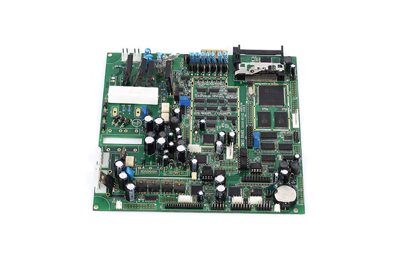
Example Of Scspcba On Pcba Design Scheme
PCBA Design LED Light Panel Lighting Application
The board includes components such as resistors, capacitors and LED chips arranged in a specific layout to control the brightness and color of the light.
PCBA Design Motor Control Board Application
Used in applications such as robotics and automation to control the speed and direction of motors. Such motor boards typically include components such as microcontrollers, drivers, and power management circuits.
PCBA Design Audio Amplifier Board Application
Consists of components such as operational amplifiers, capacitors, and resistors arranged in a specific layout to amplify and filter audio signals.
PCBA Design Microcontroller Board Application
Examples include IoT devices and home automation. Includes microcontrollers, memory, input/output interfaces, and other circuitry needed to control and communicate with other components.
PCBA Design Power Board Application
The power board is used to provide regulated power for various electronic devices. Includes components such as transformers, rectifiers, capacitors and voltage regulators arranged in a specific layout to provide a stable and reliable power supply