HOME /Products /PCBA Services /DFM Inspection
☑ PCB Assembly Services
☑ ISO9001 & UL Certified
☑ Instantly Quote & Order Today
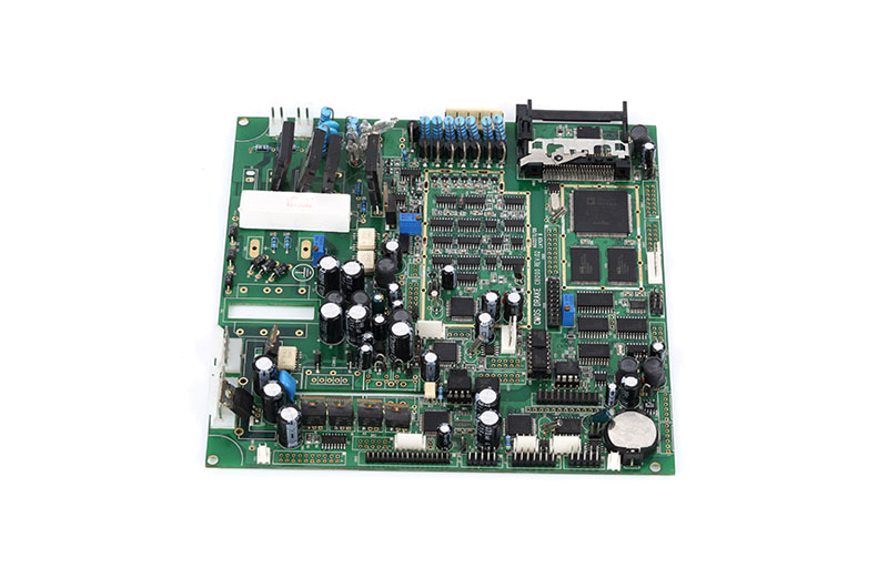
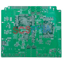
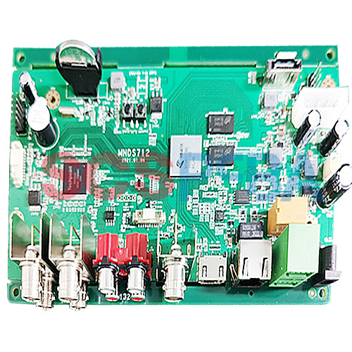
SCSPCBA is committed to providing global customers with samples and one-stop electronic manufacturing services for small and medium batches. PCBA DFM inspections can be performed by SCSPCBA to ensure your PCBs are manufactured correctly and increase the reliability of your products.
Before PCBA production, we will conduct a DFM inspection on customer design documents to ensure the quality of the manufacturing process, provide professional DFM reports, and may partially modify the design
DFM Inspection Application Scenarios
SCSPCBA in DFM inspection mainly has four aspects, namely circuit board design, component layout, soldering process, and board testing issues
Circuit Board Design
In circuit board design, DFM inspection can check whether the board meets the manufacturing standards. For example, we check the board for issues such as too small holes or too dense a component layout to ensure that the board can perform properly during the manufacturing process.
Component Layout
Component layout refers to in. DFM inspection can check whether the position and layout of components placed on the circuit board comply with PCBA manufacturing standards. For example, we check for issues such as overcrowded component placement or incorrect component placement to ensure components can be soldered correctly.
Soldering Process
During the soldering process, DFM inspection can check whether the PCBA soldering process meets the manufacturing standards. For example, check whether there are problems such as short circuits or sparking during the welding process to ensure the quality and stability of the welding
Board Testing Issues
After a board is manufactured, it needs to be adequately tested to ensure that it is functioning properly and that all components are properly seated. This reduces production issues and improves board quality and reliability.
Drill Inspection
During PCB manufacturing, drilled holes provide access for electronic components to connect to the surface of the PCB. Therefore, during DFM inspection, drill inspection analysis is an important step to ensure PCB quality.
| Drill Inspection | Inspection Analysis |
| Drill Hole Size | If the size of the drill holes is not as required, the electronic components may not be properly connected to the PCB, resulting in connection failure or malfunction |
| Drill Hole Location | If the drill holes are not in the correct position, the electronic component may be placed unstable, causing other components on the PCB surface to not fit properly |
| Drilled Copper Plated | Drilled holes are plated with copper to ensure the conductivity of the holes. If the copper plating on the drill holes is insufficient or uneven, the electronic components may not be properly connected to the PCB, resulting in connection failure or malfunction |
| Drilling Depth | If the holes are not deep enough or too deep, the electronic components may not be properly connected to the PCB, resulting in connection failure or malfunction |
| Use X-ray Inspection | Non-contact method for checking that holes are correctly positioned and oriented |
Solder Mask Checks
A solder mask is a layer of polymer coated on the surface of the PCB to protect the copper wires from oxidation and prevent short circuits. The solder mask also serves as a visual aid for identifying components on the PCB.
|
Solder Mask Checks Inspection |
Inspection Analysis |
|
Solder Mask Coverage |
The solder mask should completely cover the copper traces to prevent oxidation and short circuits. Any areas not covered by the solder mask should be identified and corrected |
|
Solder Mask Alignment |
The solder mask should be aligned with the copper traces to prevent misalignment during soldering. Misalignment can lead to poor solder joints and ultimately affect the functionality of the PCBA |
|
Solder Mask Fragments |
Solder mask chips are small pieces of solder mask that come off during the manufacturing process. This debris can cause short circuits and should be identified and removed |
Signal Inspection ensures that the signals on the PCB are properly routed and meet the design requirements. It uses a range of techniques such as netlist comparison, simulation, and visual inspection.
|
Signal Inspection |
Inspection Analysis |
|
Netlist Comparison |
Comparing the design netlist with the netlist generated during the PCB layout process. Any differences between the two netlists could indicate an error in the routing of the signal |
|
Simulation |
Running simulations to check the electrical characteristics of the signal. This helps to identify issues such as signal integrity problems, crosstalk, and timing issues. |
|
Visual Inspection |
Involves visually inspecting the PCB to check that the signal routing is correct and that there are no issues such as incorrect placement of components or damaged traces. |
|
Mixed Layer Inspection |
Inspection Analysis |
|
X-ray Inspection |
Using X-rays to inspect the internal layers of the PCB. This is particularly useful for checking the alignment of the layers and the quality of the vias. |
|
Visual Inspection |
Inspecting the PCB to check that the layers are properly aligned and that there are no issues such as misplaced vias or damaged traces |
|
Electrical Testing |
Testing the electrical characteristics of the PCB to check for any issues such as short circuits or open circuits. |