HOME /Products /PCB Services /PCB Design
☑ Over 10 Years of Experience
☑ Quote With 24 Hours
☑ PCBA Manufacturer
☑ OEM Supplier
☑ PCB & PCBA Welding Services
☑ Fast PCB Assemble
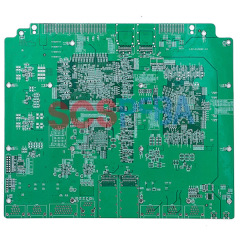
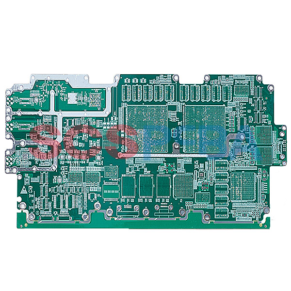
PCB (Printed Circuit Board) design refers to the process of creating a printed circuit board layout, including schematic capture, component placement, electrical connection routing, and design rule checking.
PCB Design Method
SCSPCBA mainly uses three methods in designing PCB:
Manual PCB Design
Manual PCB layout is designed manually using pen and paper, or specialized PCB design software
Manual PCB design is suitable for small and simple designs but is time-consuming and error-prone
Automatic PCB Design
Automated PCB design is the method of automatically routing connections on a PCB layout using software
This approach saves time and effort in designing large and complex boards, but the final layout may not be optimal and adjustments may be required
Hybrid PCB Design Approach
The hybrid approach combines manual design and automatic routing
SCSPCBA professional pcb designers manually place critical components and manually route high-speed and sensitive connections while routing the rest using the auto-routing function
A hybrid PCB approach can provide the best of both worlds by enabling optimal routing while reducing overall design time
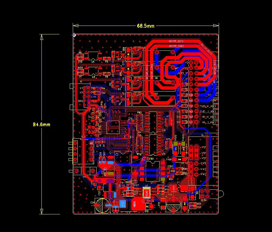
Printing Circuit Board Drawing
A PCB drawing, also known as a PCB schematic diagram desing, is a visual representation of a printed circuit board (PCB) and its components. It usually includes information such as the location, orientation, and polarity of components on the board. Here are some common elements that might be included in a PCB assembly drawing:

Component Placement
The diagram will show the location and orientation of each component on the board. This may include information such as part number, value and polarity.
Printed Circuit Board Layout
This image will show the layout of the PCB, including the locations of traces, vias, and mounting holes. This information may be helpful during assembly.
Soldering Instructions
The diagram may include instructions on how to solder each component to the board. This may include information such as recommended soldering temperature, amount of solder to use, and duration of the soldering process.
Test Point
The diagram may include test points on the board that can be used to check the functionality of the board during the testing phase.
Mechanical Details
This drawing may include mechanical details such as board dimensions, mounting hole locations, and any other relevant information that may be required during assembly.
Overall, a PCB assembly drawing is a useful tool in ensuring that a PCB is assembled and functioning properly. It helps reduce errors during assembly and can be used as a reference during testing and troubleshooting.
How to Get Started with PCB Design
Starting a PCB (printed circuit board) design project can seem daunting, but it can be an enjoyable and rewarding experience if approached the right way. Here are the steps to start PCB design:
Define Project Requirements
Before starting a design, it is important to define project requirements, including what the PCB will be used for, the types of components to be used, and the required size and shape.
Choosing Design Software
There are many free and paid PCB design software options available. Some popular options include Eagle, Altium Designer, and KiCad.
Creating A Schematic
The schematic is the first step in designing a PCB. It shows the connections between components and helps identify any potential design issues.
Create the PCB Layout
Once the schematic is complete, the next step is to create the PCB layout. This involves placing components on the PCB and routing connections between them.
Verify Design
Before sending design files for manufacturing, it is important to verify the design for any errors or issues. Most PCB design software includes tools for validating designs, such as design rule checking (DRC).
Generate Manufacturing Files
After the design is verified, the next step is to generate manufacturing files. These files include Gerber files, which contain the design information needed to manufacture the PCB.
Send Files for Fabrication
Finally, the fabrication files are sent to the PCB manufacturer for production.
Remember, PCB design is a skill that takes time to develop. Don't be afraid to ask for help or consult online resources and forums to improve your skills.
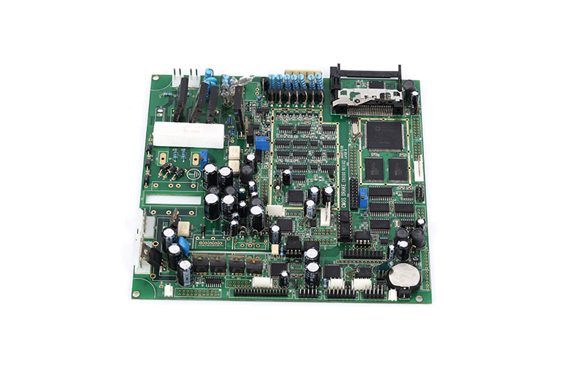
Provide a small control board pcb design with simple functions and easy operation:
The main functions of this small control board:
The power supply is 24V, which is converted into 5V and 3.3V by the power chip for the whole circuit.
4-way relay output to control peripheral equipment, such as contactors, motors, etc.
The 8-way IO input needs to be designed for electrical isolation, and there is a common terminal for PNP and NPN switching.
One CAN communication interface to communicate with the industrial computer.
4-bit DIP switch for CAN ID setting.
Scspcba has completed the design of the pcb, and there is no need to find other manufacturers for proofing. We are a one-stop service provider, and we can make samples by ourselves and debug the samples. Similarly, if our customers need to add functions to this board, scspcba can also provide corresponding functional designs
Is PCB a CAD design?
Yes, PCB (Printed Circuit Board) design is a type of CAD (Computer Aided Design) software used to design electronic circuits and printed circuit boards. PCB design software allows designers to create schematics, define board layouts, and perform routing to connect the various components on the board. PCB design software also provides tools for validating designs, generating manufacturing files, and interacting with PCB manufacturers. So, in short, PCB design is a specific type of CAD design that focuses on designing and producing printed circuit boards.