Printed circuit board (printed circuit board, PCB) is to fix various components in the circuit, provides a connection circuit between various components and is made of a material with insulation and heat insulation and a certain strength. In a broad sense: It is a finished product that is equipped with electronic components such as LSI, IC, transistors, resistors, capacitors, etc. on a printed circuit board, and sent to electrical communication by soldering. In a narrow sense: it is a semi-finished board with no components installed and only wiring circuit graphics, which is called a printed circuit board.
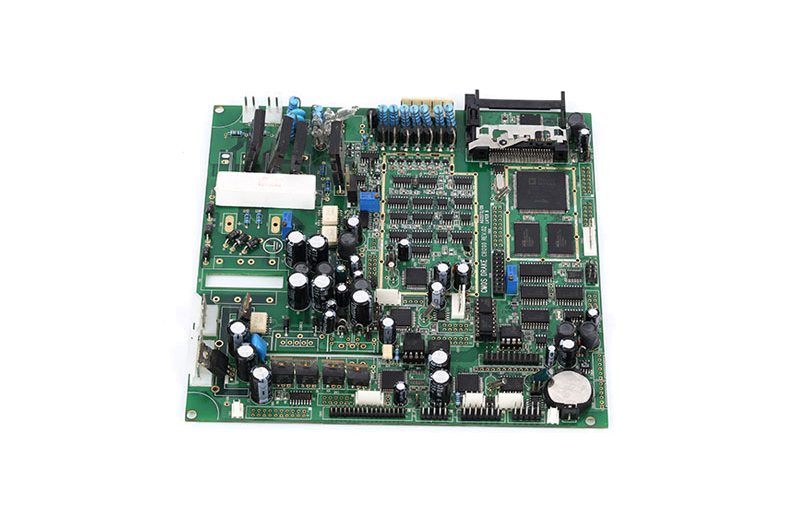
PCB is an essential circuit carrier for all electronic products, widely used in communication electronics, consumer electronics, computers, automotive electronics, industrial control, medical equipment, national defense and aerospace and other fields.
The exposure process plays a vital role in PCB manufacturing, it is one of the key steps to transferring the design pattern to PCB surface. The exposure process transfers the design pattern from the drawing or CAD file of the circuit board onto a light-sensitive material (photoresist). These patterns define the wires, electrical components, and other important structures on the board. The exposure process ensures that the design is accurately and precisely transferred onto the PCB substrate, thereby laying the groundwork for subsequent process steps.
As the size of electronic devices becomes smaller and smaller, the lines and components on the PCB become smaller and smaller. The exposure process can achieve high resolution and transfer fine pattern details to the PCB, thus meeting the needs of modern electronic devices for dense circuit layouts.
Complex PCBs may have multiple layers, each layer containing different circuit components and wires. The exposure process ensures precise matching of pattern positions between different layers through layer-to-layer alignment for proper connection and function in stacked-layer PCBs.
The ability to automate and control the exposure process ensures consistent results in mass production. This consistency is critical to ensuring that all produced PCBs meet design specifications as well as functional requirements.
The photoresist used in the exposure process must have the appropriate chemical and physical properties to allow for accurate pattern transfer during exposure. Optimizing the exposure process also involves selecting the correct photoresist and determining the appropriate exposure parameters.
The exposure process is usually a relatively rapid step in the PCB manufacturing process, and the transfer of the pattern can be completed in a relatively short time. This helps improve overall productivity and throughput.
With the development of technology, the exposure process is also constantly innovating. The new exposure technology and equipment can better meet the requirements of high density, high resolution and fine feature preparation, and promote the continuous advancement of PCB manufacturing technology.

Optimizing the exposure process plays a key role in obtaining high-quality PCBs
PCB exposure equipment is a device that transfers pre-prepared circuit image information to copper substrates through photolithography technology. It is a comprehensive product integrating electrical automation, microelectronic control, mechanical design, optoelectronics, vacuum sealing, and CCD alignment. . Exposure equipment is the concentrated carrier of lithography technology and the most important process link in lithography technology. It determines the quality of the circuit diagram of PCB products and the overall performance of the product. It is one of the key equipment in PCB manufacturing.
Classification of PCB Exposure Equipment
In the PCB manufacturing process, PCB exposure equipment is required for the inner layer image, outer layer image and solder mask. Therefore, according to the PCB manufacturing steps, exposure equipment can be divided into exposure equipment for circuit layers and exposure equipment for solder mask layers.
The circuit layer is the basic core layer of the PCB, responsible for connecting and transmitting electrical signals between electronic components. During PCB processing, the processing accuracy and quality of the circuit layer directly affect the performance and reliability of the entire circuit board. In most PCB designs, the number of circuit layers is generally large, such as multilayer boards, each board contains multiple electronic components that need to be connected. Therefore, the demand for circuit layer exposure equipment is relatively large. The main functions and features of exposure equipment for PCB circuit layer include:
The exposure equipment is equipped with an appropriate light source, usually a UV lamp. These light sources generate high-energy UV light that is used to expose light-sensitive photoresists.
The mask (or mask) that controls the pattern transfer is placed between the light source and the PCB. The transparent and opaque areas on the mask match the desired PCB trace pattern.
Exposure equipment is usually equipped with an alignment system to ensure accurate alignment between the PCB substrate and the mask. This is critical for the accuracy of layer-to-layer alignment and line placement.
Operators can adjust parameters such as exposure time and light intensity to obtain the best exposure effect according to different photoresists and PCB materials.
Solder mask effectively improves PCB stability
In the PCB manufacturing process, the solder mask is a protective layer covering the surface of the circuit board. It can protect the circuit copper foil from the external environment and play a role in fixing components and circuit connections. PCB solder mask exposure equipment plays a key role in the PCB manufacturing process, which ensures the quality and accuracy of the solder mask on the surface of the circuit board, thereby improving the stability and reliability of the PCB. The main functions and features of exposure equipment for PCB solder masks include:
Similar to the exposure equipment for the circuit layer, the exposure equipment for the solder mask layer also needs an appropriate light source to generate sufficient ultraviolet light energy.
· Masking System
Masks for solder resistance typically include areas to be protected that will not be cured by the photoresist. The transparent areas of the mask match the solder mask pattern.
The alignment system ensures accurate alignment between the photoresist and the mask so that the solder resist pattern is correctly transferred to the PCB surface.
The control and adjustment of exposure parameters also play an important role in solder mask exposure equipment to ensure the quality and consistency of solder mask patterns.

Expose Equipment Determines The Quality of The PCB Product Circuit Diagram And The Overall Performance of The Product
In PCB manufacturing, the parameter setting of the exposure process is a key factor, which directly affects the pattern transfer and the quality of the final circuit board.
Exposure time refers to the length of time that the PCB is exposed to the light source in the exposure equipment. Generally speaking, the exposure time should not be too short to ensure that the photoresist has enough time to cure. However, it should not be too long to avoid loss of pattern details or excessive curing of the adhesive layer due to overexposure.
Light intensity refers to the energy density of the exposure light source, usually measured by the light energy per unit area. Too low a light intensity may result in the under-curing of the photoresist, while too high a light intensity may cause over-curing of the bond line or thermal effects.
Photoresist thickness refers to the thickness of the photoresist coated on the surface of the PCB. Too thin an adhesive layer may lead to unclear patterns after exposure, while too thick an adhesive layer may lead to increased exposure time.
The best choice of exposure parameters usually needs to be determined through experimentation and optimization. In the PCB manufacturing process, small batch experiments can be carried out, trying different parameter combinations, and then selecting the best parameters by checking the quality of the cured pattern. Real-time monitoring during the manufacturing process can also help in parameter adjustment and optimization.

PCB Circuit Board Exposure Solder Resist Exposure
PCB exposure process is a vital part in the electronic manufacturing industry. It is used to manufacture various types of circuit boards, including conventional rigid circuit boards, flexible circuit boards, multilayer circuit boards, and high-density interconnection boards. Through the exposure process, complex circuit patterns can be transferred to different levels to realize the connection and function of electronic devices.
Whether it is a mobile phone, a network router or a communication base station, high-quality PCBs are required as core components. The exposure process plays an important role in the manufacture of communication equipment, ensuring the transmission of high-frequency signals and the reliability of circuits.
Consumer electronic products such as flat-panel TVs, smartphones, audio equipment, etc. all rely on high-quality PCBs. The exposure process ensures that the electronic components and circuits of these devices work accurately and reliably.
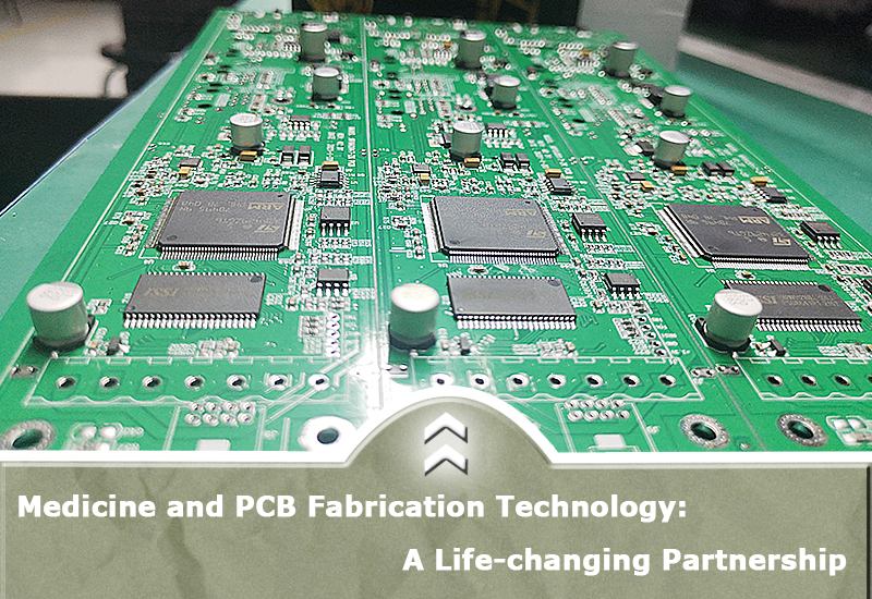
Medical equipment requires high precision and stability, so the application of PCB in medical equipment manufacturing is crucial. The exposure process helps to manufacture high-precision circuit boards for medical imaging, monitoring equipment, diagnostic instruments, etc.
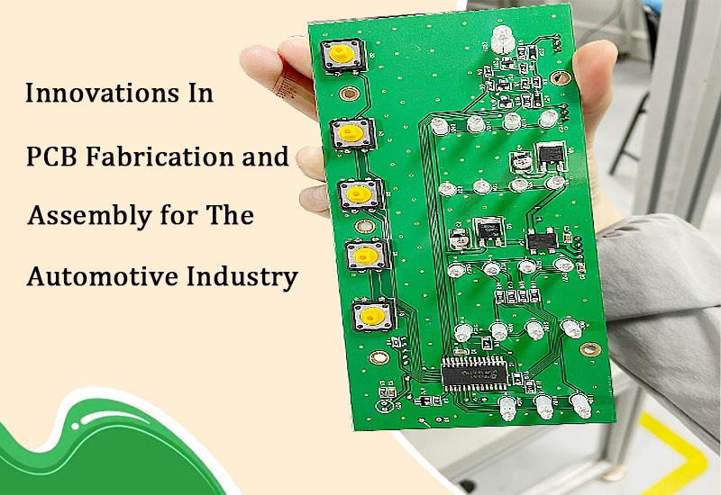
Many functions in modern vehicles rely on complex electronic systems such as engine controls, safety systems, entertainment systems, and more. Exposure processes are used to manufacture PCBs in automotive electronics, ensuring the performance and stability of these systems.
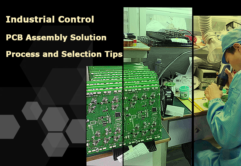
The field of industrial automation requires high-performance electronic control systems to automate and monitor production processes. Exposure processes are used to manufacture the PCBs required for these control systems.

PCB Exposure Process Is Widely Used In Various Fields
In general, the PCB exposure process has a wide range of applications in many fields, from personal consumer electronics to highly complex industrial and scientific equipment. The needs and requirements of different fields promote the continuous innovation and development of PCB technology so that it can adapt to the needs of different application scenarios.