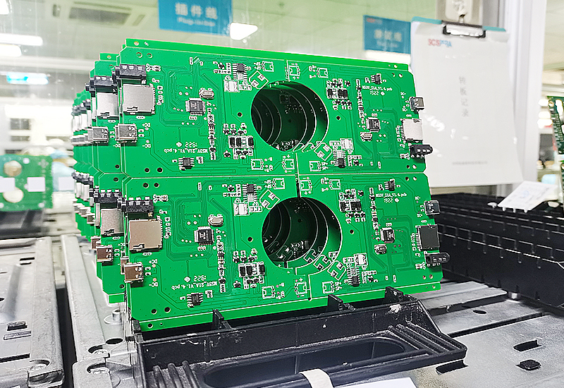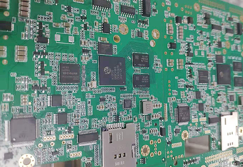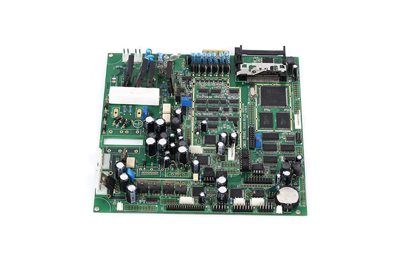
In electronic product manufacturing, printed circuit boards are widely used. They carry electronic components and connect them, and are an important part of electronic equipment. However, sometimes you may encounter issues with PCB Warpage, which can bring a series of challenges to the reliability and performance of your product.
PCB warpage is one of the common problems in the PCB fabrication process. When a PCB bends or twists during use, it is called a warpage.. This problem can cause the board to degrade or even fail. To solve this problem, we need to understand the cause and the corresponding measures. Next, we’ll dive into the causes of PCB Warpage and solutions.
● Reason: The PCB board lacks moisture-proof packaging, or is left exposed in a humid environment. Due to the large moisture absorption area of the board, warping occurs. Take copper-clad laminate as an example. If the humidity of the inventory environment is high, the moisture absorption area of the single-sided copper-clad laminate is large, which will increase warpage; the moisture of the double-sided copper-clad laminate can only penetrate from the end face of the product, the moisture absorption area is small, and the warpage changes slowly.
● Measures: Choose a suitable storage environment.
· Humidity Control: Regularly monitor the humidity of the storage environment. The humidity should be controlled between 40% and 60% of relative humidity (RH). This can reduce deformation and warping caused by moisture absorption of PCB materials. At the same time, an air conditioning system can be installed to control temperature and humidity to ensure the stability of the storage environment.
· Avoid Exposing them naked: For PCB materials without moisture-proof packaging, try to avoid direct exposure to moisture. Pack PCB materials using methods such as moisture-proof cabinets or sealed bags to reduce the possibility of moisture absorption. You can use racks or pallets to increase the distance between the PCB material and the ground to reduce the possibility of moisture absorption.

● Reason: Improper placement of PCB boards, such as vertical placement or heavy objects on the PCB board, stacked PCB boards, poor placement, etc. will increase board warpage and deformation.
● Measures: Avoid vertical or tilted placement to reduce the possibility of board warping. Placing it horizontally on a flat surface; do not place heavy objects on the PCB board; place them dispersedly and avoid placing to many PCB boards in the same area to reduce deformation caused by concentrated pressure. Also, use supports or spacers to provide support and ensure that the edges of the PCB board are not damaged or pinched.
● Reason: if the PCB design does not comply with the principles of structural strength and stability, for example, the graphics of the circuit board design are unbalanced or the circuits on both sides of the board are asymmetrical; or there is an excessive concentration of components or long-distance unsupported areas.
● Measures: When designing PCB, give priority to graphic symmetry, line balance, component selection, and division. Add support structures or strengthen circuits to increase the overall structural strength and stability, and then verify the PCB design through simulation tools to ensure that all parts of the PCB are fully supported.
● Cause: Improper process operations during processing, such as high-temperature control, large thermal shock, or excessive pressure, etc., may cause PCB material deformation, resulting in warping.
● Measures:
· Develop corresponding processing parameter standards for different PCB materials and process requirements, and strictly implement and monitor the pressure parameters of processing equipment to ensure that temperature, pressure and other parameters during the processing are controlled within appropriate ranges;
· Minimize thermal shock during processing and avoid sudden temperature changes or rapid heating/cooling processes to reduce thermal stress on the PCB material, ensure uniform temperature distribution during heating or cooling, and reduce the risk of deformation.
· Processing operators need to receive professional training, understand the operating principles and parameter-setting methods of processing equipment, and master correct processing technology to ensure the stability and controllability of the processing process.

● Reason: the PCB manufacturing process, it is exposed to heat multiple times and is exposed to a variety of chemical substances. For example, the substrate needs to be washed, dried, and heated after etching. The electroplating is hot during graphic plating. After printing logo characters, it needs to be heated and dried. These processes may cause the board to warp.
● Measures:
· Optimize the process flow, reasonably arrange the process steps, and reduce excessive heat treatment and chemical treatment processes;
· Strictly control the temperature to avoid excessive temperature, and use temperature control equipment to ensure that the temperature of heating, drying, and other processes is stable within an appropriate range. Avoid excessive temperature changes, use gentle heating methods, control heating speed, etc.
· Strengthen quality control, set reasonable process parameters for different process steps, and monitor and adjust process parameters, such as heating time, heating temperature, chemical treatment time, etc.
●Cause: When the circuit board is in the reflow oven, wave soldering or dip soldering process, if the solder temperature is too high or the operation time is too long, it will cause uneven thermal expansion and contraction of the circuit board, thereby increasing the possibility of PCB warping.
● Measures:
· Reduce the size and number of panels: To reduce the dent deformation caused by the weight of the circuit board when passing through the furnace, the size of the circuit board can be reduced as much as possible and the number of panels can be reduced. When passing through the furnace, it is best to keep the long side of the circuit board perpendicular to the direction of the reflow oven chain to reduce the amount of dent deformation.
· Use oven pallet jigs: oven pallet jigs made of high-temperature resistant materials such as aluminum alloy or synthetic stone can stabilize the circuit board and reduce deformation.
· Double-layer pallet fixture: If the single-layer pallet fixture cannot effectively reduce the deformation of the circuit board, consider using a double-layer pallet, that is, clamping the circuit board between the upper and lower pallets. This can further reduce the deformation problem of the circuit board when passing through the reflow oven.
Prev:Complete Medical-grade Printed Circuit Board Manufacturing Process
