Today, with the rapid development of electronic technology, printed circuit boards have become the top priority of all types of electronic equipment. PCB have become an indispensable core component of modern electronic equipment due to their compactness, reliability, electrical performance and other characteristics. However, there are still many people who do not know the importance of printed circuit boards. Today, we will take you to explore the importance of circuit boards in depth, from the three aspects of their structure, schematic design process, and characteristics.
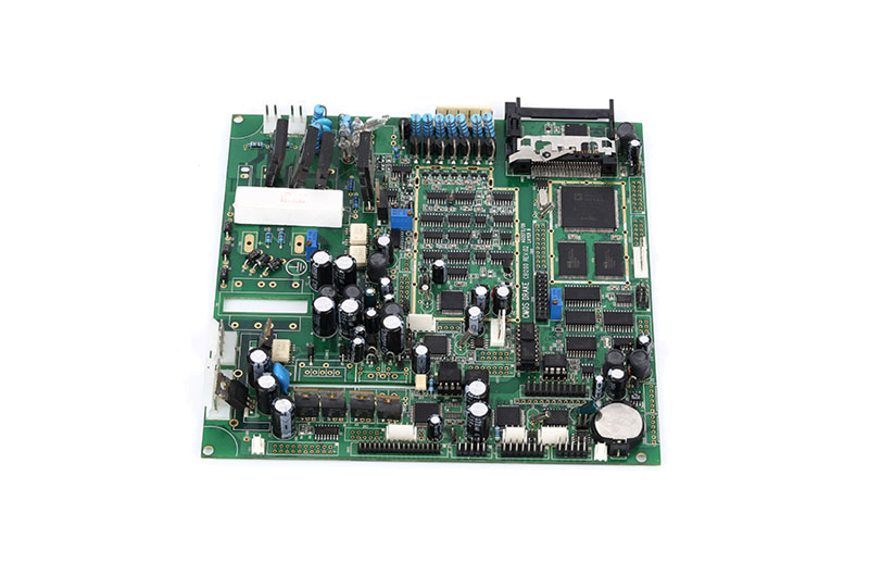
The structure of a circuit board mainly includes several key components such as pads, vias, mounting holes, wires, components, connectors, fills and electrical boundaries. Each of them performs different functions, which are explained in detail below.
The soldering pad is a metal hole specially used for soldering to connect component pins. The purpose is to ensure that the components are securely mounted on the circuit board.
There are metal vias and non-metal vias in the PCB. Metal vias are used to connect component pins between different layers to achieve overall circuit connectivity.
Used to firmly fix the PCB in a specific position to ensure the stability and reliability of the entire system.
Wires are the electrical network copper film on the circuit board, responsible for connecting the pins of various components so that the entire circuit can work properly.
The components of the PCB are the core part of the electronic equipment. They realize their functions through the pins connected to the circuit board.
Used to connect components between different printed circuit boards to achieve collaborative work of the entire system.
Filling is a form of copper coating, mainly used in ground wire networks to help reduce impedance and improve circuit performance.
The electrical boundary specifies the size of the circuit board. All components must be within this boundary to ensure the normal operation of the circuit board and the rationality of the overall design.

The working process of the PCB is to isolate the substrate insulating material covered with a copper foil conductive layer on the surface so that the current flows between various components along the pre-designed route and realizes the multiple functions of the electronic device.
On a basic PCB, the components are located on one side and the wires are concentrated on the other side. A single-layer PCB has all the wires on one side. Multilayer PCBs contain multiple wire layers, with circuit connections between different layers. The bridge connecting the circuits is called a via.
(1) Circuit schematic diagram design: Draw circuit schematics using a professional device editor
(2) Network report of circuit schematic diagram: It can display the link relationship between PCB and each component, and can quickly find the category, placement, position, and other relationships of the components, providing convenience for subsequent PCB design.
(3) Printed circuit board design: Convert the circuit schematic diagram into the final form. The design of this part is more difficult than the circuit schematic design and requires professional PCB experts or teams to complete the design function.
(4) Generate printed circuit board reports: After the printed circuit board design is completed, various reports need to be generated, such as pin reports, circuit board information reports, network status reports, etc., and finally print out the printed circuit diagram. These reports provide detailed information and an overall overview of the design.

PCB boards allow a large number of components and circuits to be highly integrated in a limited space. This compact design helps reduce the size and improve the performance of electronic devices.
The PCB assembly manufacturing process adopts automated technology, which reduces manual operations, thus improving the reliability and stability of the circuit board. At the same time, the PCB's materials and manufacturing process are carefully selected to ensure that the circuit works properly under various environmental conditions.
The PCB realizes the electrical connection between various components through structures such as wires, pads, and connections, accurately controls impedance and improves circuit performance, thus forming a complete circuit.
PCB fabrication and assembly processes are increasingly specialized and mechanized, with mass production carried out through automated equipment. This not only improves manufacturing efficiency but also reduces manufacturing costs.
Printed circuit boards support and fix various electronic components, such as resistors, capacitors, integrated circuits, etc., through welding or plug-in methods.
PCB is flexible and can be single-sided, double-sided, or multi-layer. Engineers can design and select according to specific application requirements. Multilayer boards can provide more wiring space, and components at different levels can be arranged at different levels to meet the requirements of complex circuits.