The Surface Mount Technology patch process is an integral part of modern electronics manufacturing. It involves the use of automated machines to place electronic components onto a printed circuit board. Proper component sourcing, board preparation, solder paste application, accurate component placement, and thorough inspection and testing are critical to ensuring a successful and efficient PCBA process. By strictly following these steps, manufacturers can produce high-quality, reliable electronic devices that meet market demands.
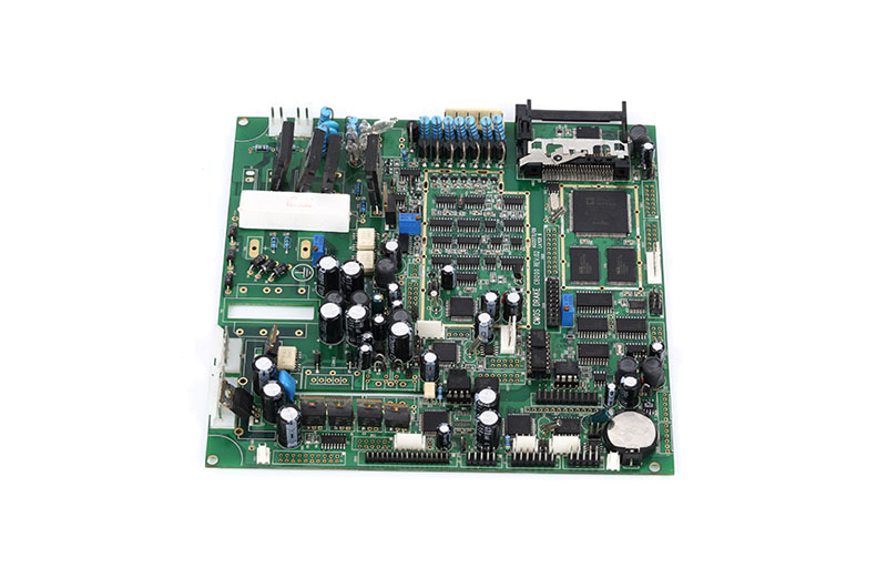
In the field of electronic manufacturing, PCBA plays a vital role. The process involves mounting SMT components onto a circuit board, however, before the actual installation, several steps need to be taken to ensure that the PCB assembly process is successful and efficient.
The first step in preparation before SMT mounting is to purchase all necessary electronic components. This is a crucial step while components are inspected and tested to verify quality and functionality.
The circuit board needs to be cleaned and inspected to make sure it is free of dust, debris, or any defects that could affect the installation process.
Solder paste is a critical component in the SMT mounting process as it acts as the adhesive that secures the component to the circuit board. Solder paste should be applied carefully and accurately to ensure proper component alignment and connection.
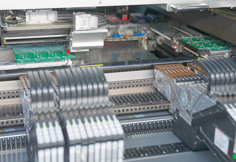
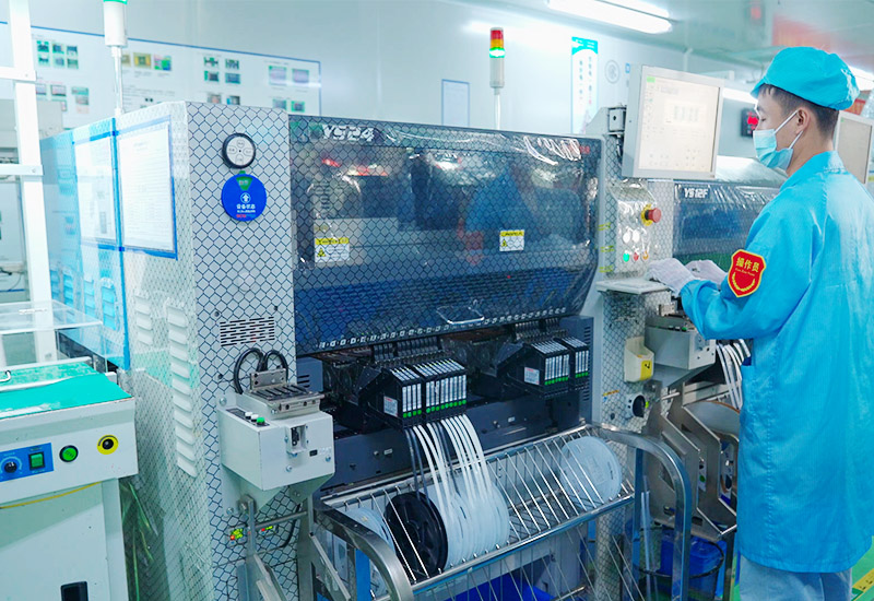
Specialized placement machines are used to precisely position each component to its designated location on the circuit board. The accuracy and precision of the placement machine are crucial to ensure that components are installed correctly without any misalignment or damage.
An automated optical inspection (AOI) machine is used to check for any defects or errors during installation. Any discrepancies or problems discovered during the inspection should be dealt with and resolved promptly to ensure high-quality and reliable products.

Solder paste printing is a technology that deposits solder paste precisely onto PCB pad locations. Apply the solder paste to the circuit board using a stencil with the stencil cutouts corresponding to the locations of the solder paste on the PCB.
High-quality solder paste printing is critical to the overall performance and reliability of PCB assemblies. Solder paste must be deposited accurately and evenly on the pad locations to ensure correct solder joints are formed during the subsequent reflow soldering process. The solder paste printing process is also affected by factors such as the type of solder paste used, the thickness and design of the stencil, the pressure and speed of the squeegee, and the temperature and humidity conditions of the printing environment. All these factors need to be carefully controlled and optimized.
To achieve this goal, SCSPCBA PCB assembly machines use advanced equipment such as automated optical inspection (AOI) systems to ensure that solder paste is deposited at designated locations and any deviations or defects are detected and corrected before the assembly process continues.
Poorly printed solder paste can cause defects such as solder bridging, insufficient solder volume, or component misalignment. These defects can result in incorrect connections, electrical shorts, or failures in the final product, resulting in serious quality issues and costly rework.
Correct and precise placement of components in SMT patches is crucial to ensure PCB assembly manufacturing and functionality. Any misalignment or incorrect placement may cause the device to malfunction or not function properly. Therefore, one should ensure that the components are compatible with the PCB design and meet the required specifications. The size, shape, and lead configuration of the component must align with the corresponding pads on the PCB.
To achieve precise component insertion, various advanced technologies and equipment are used. These machines use vision systems to detect the position and orientation of components and place them accurately on the PCB. This automated process not only saves time but also ensures consistent and reliable results.
Once the components are placed on the PCB, they need to be firmly connected using solder. This soldering process requires heat to melt the solder and create a strong bond between the component leads and the PCB pads. This step is crucial as it ensures good electrical conductivity and mechanical strength.

When components are not placed correctly on the PCB, it can lead to poor connections and ultimately failure of the electronic device.
Component misalignment can be caused by a variety of factors, such as incorrect machine settings or human error. To mitigate this problem, ensure that the machine is properly calibrated and the operator is trained to accurately place components onto the PCB.
Solder is used to create the connection between the component and the PCB. However, defects such as solder paste residue or insufficient solder paste can compromise the integrity of these connections.
This results in poor electrical conductivity or even complete failure of the electronic device. To minimize soldering defects, the solder paste application process must be carefully monitored and the reflow soldering parameters must be set correctly.
Solder paste is typically applied to the PCB using a stencil such as a steel mesh. If the steel mesh is not properly aligned or the solder paste deposition is inconsistent, it can result in bad solder joints.
To combat this problem, stencils should be inspected regularly, automated inspection systems should be employed, and proper cleaning procedures should be implemented to maintain high-quality printing.
Prev:Do You Have Questions About PCBA Chip Components? Read This!
Next:Master PCBA Manufacturing with These 8 Useful Soldering Tips
