The circuit board (PCB) manufacturing process begins with the production of engineering information, which allows engineers to optimize the circuit board design so that it is easier to manufacture during the production process and can meet customer performance and quality standards. This is the first step in circuit board manufacturing and lays a solid foundation for subsequent manufacturing processes.
First, engineers communicate with customers to understand their needs and specifications in detail. This includes requirements for circuit function, size, performance parameters, etc.
Based on understanding the customer's needs, engineers begin to design the original layout of PCB. They select appropriate components and determine their layout to minimize noise, cross-interference, and other potential problems with the circuit. This also includes optimizing circuit performance.
After determining the layout of the circuit, engineers proceed with wiring planning. This is the process of connecting electronic components to each other and to external interfaces. Cabling needs to consider factors such as signal transmission, power supply, and ground connections.
Engineers will select appropriate circuit board materials, number of layers and copper foil thickness according to design requirements. This ensures that the board meets specific electrical performance and mechanical requirements.
Finally, engineers will clearly define the requirements for the manufacturing process, including final size, number of layers, hole size, mounting hole locations, etc., to ensure that the circuit board can be manufactured smoothly and meet customer expectations.

In the manufacturing process of circuit boards (PCBs), converting circuit designs into actual circuit boards is a key link. Each step requires a high degree of precision and engineering to ensure the final PCB meets performance, quality and reliability requirements. Once the PCB is manufactured, it can be used for the assembly of electronic devices.
The first step in PCB manufacturing is to prepare raw materials. The main materials commonly used include fiberglass cloth substrates and copper foil. These materials need to be cut and prepared according to design specifications for use in subsequent processes.
The next critical step in manufacturing PCB is to transfer the circuit design pattern to the substrate. This is usually done using photolithography techniques. A light-sensitive coating is applied to the substrate, a pattern of the circuit design is then placed on the substrate, and UV light is used to transfer the pattern to the coating.
After patterning, the unnecessary copper foil is removed from the substrate through an etching process. This step uses chemical solutions or mechanical means to remove excess copper, leaving the conductor pattern required for the design.
For circuits that need to connect different layers, holes are drilled at appropriate locations. These holes are typically used to connect different layers of circuitry via holes (PTHs) or blind vias (blind vias).
Surface treatment is to improve the welding performance and protect the circuit board. This may include metallization, tin plating, or other surface coating processes.
Print logos, text and symbols as well as necessary reference information on the PCB for identification during assembly.
The last step in PCB manufacturing is to prepare it for assembly. This includes adding a solder mask to the board to protect the lines and installing surface mount (SMT) components where needed.

Once PCB are manufactured, they are typically considered semi-finished products.
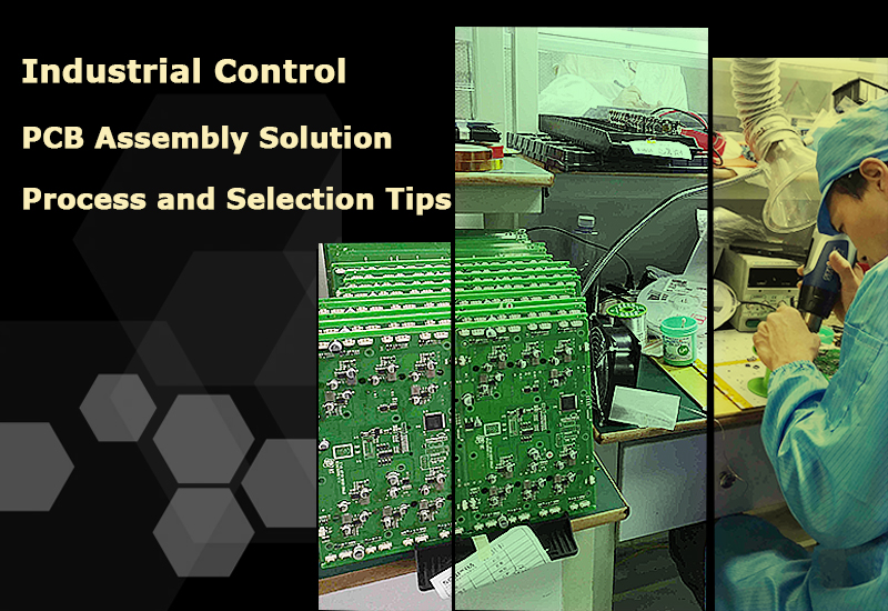
The first step in PCB assembly is to weld electronic components (such as resistors, capacitors, integrated circuits, etc.) to the circuit board. This can be done with hand soldering or automated surface mount (SMT) equipment. Soldering is a critical step because good quality soldering ensures that the circuit's connections are tight and there are no shorts.
After welding is completed, perform a visual inspection to check whether the welding is correct. Workers use magnifying glasses or automated optical inspection systems to inspect the integrity, location and quality of solder joints.
Electrical testing is performed to ensure the proper functioning of the circuit. This includes a continuity test to check that there are no breaks or shorts in the circuit. Test equipment applies voltage and current to simulate different operating conditions to ensure circuit stability and performance.
After electrical testing, functional testing is performed to verify that the circuit is working properly according to the design specifications. This usually involves applying different signals to the circuit and checking that the output is as expected.
After testing is completed, a solder mask layer is usually applied to the PCB. The solder mask is used to protect the circuit, reduce the impact of environmental factors on the circuit, and provide mechanical support.

When circuit boards (PCBs) pass through the assembly and testing stages, the ultimate goal is to transform them into finished products that meet quality standards. Only products that pass the inspection will be deemed as qualified finished products and can be put into the market or used for the assembly of electronic equipment. These quality control measures are critical to ensuring the stability and reliability of electronic devices.
Final inspection usually begins with a visual inspection. Staff will carefully inspect the outside of the circuit board to ensure there is no obvious damage, dirt or defects. This includes checking the integrity of printing, markings, welding and coatings.
All inspection and test results must be recorded to establish product quality records. These records are important for tracking and improving the manufacturing process.
For certain applications, such as military or industrial fields, environmental testing may be required to ensure that the circuit board can operate properly under extreme temperature, humidity, or vibration conditions.
In some cases, long-term reliability testing is performed to simulate the performance of the circuit board during its service life. This helps ensure long-term product reliability.

When the PCB passes production, assembly and final inspection and reaches a finished product level that meets quality and performance standards, the product is sealed and packaged and placed in the waiting area for express delivery!
Prev:Explore Wearable Devices PCB Assembly Manufacturing
Next:The Cost Is Expensive, Why Choose Rigid-flex PCB Board?