PCB (Printed Circuit Board) As the core component of modern electronic products, PCB plays a vital role in connecting and supporting electronic components. However, to ensure the performance, reliability and long life of PCBs, besides the design and manufacturing process, surface treatment also plays a key role. In PCB manufacturing, surface treatment is the application of specific chemical treatments or coatings to the surface of a circuit board to improve its performance and reliability. The surface treatment method of PCB is designed to improve the solderability, corrosion resistance, electrical performance and overall stability of the circuit board. These treatments can have an impact on soldering, electrical conductivity, corrosion resistance, etc., thus making PCB suitable for different application fields, such as communication, consumer electronics, automotive, medical, etc.

Electronic components are usually attached to the PCB by soldering. Different surface treatments can increase the wettability of the solder joint, ensuring that the solder can be well bonded to the pad and solder paste, thereby improving soldering quality and reliability.
Printed circuit boards may be affected by environmental factors such as humidity and chemicals. The surface treatment method can form a protective coating or metal layer on the surface of the PCB to enhance its corrosion resistance and prolong the service life of the PCB.
Different surface treatments can affect the quality of electrical connections, including signal transmission stability and electrical conductivity. Good surface treatment can reduce the resistance of electrical connections and improve the quality of signal transmission.
Some surface treatments use environmentally friendly chemicals to reduce environmental impact. This helps push the PCB electronics industry in a more sustainable direction.
● Principle
The process of coating molten tin-lead solder on the surface of the PCB and leveling (blowing) it with heated compressed air to form a coating that resists copper oxidation and provides good solderability.
● Steps
Clean pad surface → Apply solder paste → Preheat and solder → Hot air blowing.
● Scope of Application
Strong versatility, suitable for a variety of applications, not suitable for high-frequency applications.
● Advantages
(1) Provide good welding performance, relatively low cost
(2) Expose the PCB to a temperature of 260°C to reveal potential delamination issues
● Disadvantages
(1) Not suitable for applications requiring high-frequency performance and may cause flatness issues.
(2) The pads processed by HASL technology are not flat enough, and the coplanarity cannot meet the process requirements of fine-pitch pads. This is because the surface flatness of the tin plate is poor. Tin balls are easy to produce during PCB processing, and short circuits are more likely to be caused by fine-gap pin components. When used in a double-sided SMT process, this is because the second side has undergone a high-temperature reflow soldering, and it is very easy to remelt the tin spray to produce tin beads or similar water drops that are affected by gravity and become spherical tin spots that drop, causing surface It is more uneven and affects welding problems.
(3) Not environmentally friendly, lead is harmful to the environment

Printed Circuit Boards with HASL/Free HASL Surface Treatment
ENIG chemically coats the copper surface with a thick layer of nickel-gold alloy with good electrical properties and can protect the PCB for a long time. The deposition thickness of nickel in the inner layer is generally 120~240μin (about 3~6μm), and the deposition thickness of gold in the outer layer is generally 2~4μinch (0.05~0.1μm). Unlike OSP, which is only used as an anti-rust barrier layer, it can be useful and achieve good electrical performance during the long-term use of the PCB. In addition, it also has environmental tolerance that other surface treatment processes do not have.
● Principle
A layer of chemical nickel is first deposited on the pad, and then immersed in a gold solution to form a layer of gold.
● Steps
Clean pad surface → electroless nickel deposition → gold immersion plating → cleaning.
● Scope of application
Suitable for high-frequency applications and high-demand electrical performance.
● Advantages
(1) The PCB surface treated by ENIG is very smooth and has good coplanarity, which is suitable for the key contact surface.
(2) ENIG has excellent solderability, and the gold will quickly melt into the molten solder, and the solder and Ni form a Ni/Sn metal compound.
● Disadvantages
(1) The process is complicated, and the process parameters need to be strictly controlled to achieve good results
(2) It is easy to cause a "black pad". This is where phosphorus builds up between the nickel and gold layers. This can cause breakage and wrong board connections

Printed Circuit Board with ENIG (Electroless Nickel Immersion Gold ) Surface Finish
Compared with nickel-gold, ENEPIG has an extra layer of palladium between nickel and gold. In the deposition reaction of replacing gold, the electroless palladium layer will protect the nickel layer from being excessively corroded by the replacing gold, and palladium prevents the replacement reaction. At the same time, it is fully prepared for immersion gold. The thickness of nickel deposition is generally 120~240μin (about 3~6μm), and the thickness of palladium is 4~20μin (about 0.1~0.5μm). Gold deposition thickness is generally 1~4μin (0.02~0.1μm)
● Principle
By depositing chemical nickel, palladium and gold, a multilayer gold layer is formed.
● Steps
Chemical nickel deposition → palladium deposition → gold immersion plating → cleaning.
● Scope of Application
High-frequency, high-reliability applications with high requirements, such as aviation and military.
● Advantages
Offers very high flatness, electrical performance, and corrosion resistance for high-end applications
● Disadvantages
Palladium is expensive and is a scarce resource. At the same time, like nickel-gold, its process control requirements are strict.
 Surface Finish")
Printed Circuit Board with ENEPIG (Electroless Nickel Electroless Palladium Immersion Gold ) Surface Finish
● Principle
An organic solder-protective layer is formed on the surface of the pad to protect the pad from oxidation.
● Steps
Clean pad surface → Apply organic solder mask → Dry and cure.
● Scope of Application
It is estimated that about 25%-30% of PCBs currently use the OSP process, and the proportion has been rising (it is very likely that the OSP process has now surpassed tin spraying and ranks first). The OSP process can be used on low-tech or high-tech PCBs, such as PCBs for single-sided TVs and boards for high-density chip packaging. For BGA, there are many applications of OSP. If the PCB has no surface connection functional requirements or storage period limitations, the OSP process will be the most ideal surface treatment process.
● Advantages
Environmental protection, suitable for small batch production, has all the advantages of bare copper plate welding, expired (three months) boards can also be resurfaced, but usually only once.
● Disadvantages
(1) Poor corrosion resistance and heat resistance.
(2) Vulnerable to acids and humidity. When used for secondary reflow soldering, it must be completed within a certain period of time, and usually the effect of the second reflow soldering will be relatively poor. If the storage time exceeds three months, it must be resurfaced. Use within 24 hours after opening the package. OSP is an insulating layer, so the test point must be printed with solder paste to remove the original OSP layer in order to contact the pin for electrical testing.

Printed Circuit Board with OSP / Entek Surface Finish
● Principle
The principle of Immersion Silver is to deposit a thin layer of silver on the surface of the PCB borad. This layer of silver can improve the conductivity of the pad, making it more suitable for high-frequency signal transmission. In addition, silver has good wettability, which can improve soldering quality and ensure good bonding of solder to pad.
● Steps
Clean the pad surface to make sure it is free of dirt and oxides.
A layer of silver plating is formed on the surface of the pad, usually by soaking the PCB in a silver solution.
Wash to remove excess silver solution and other impurities.
● Scope of Application
The immersion silver method is widely used in electronic equipment for high-frequency and high-speed signal transmission, such as communication equipment, computer motherboards, high-speed data transmission equipment, etc. Due to silver's high conductivity and excellent signal transmission performance, immersion silver can improve the signal quality and reliability of the circuit board.
● Advantages
(1) High Conductivity: Silver is an excellent conductive material and can provide a low-resistance connection.
(2) Excellent signal transmission: Immersion silver can reduce the loss in signal transmission and improve the quality of signal transmission.
(3) Silver has good wettability, which helps to improve soldering quality.
(4) High-temperature stability: Silver has good stability under high-temperature conditions and is suitable for some high-temperature environments.
● Disadvantages
(1) Environmental Sensitivity: Silver may react with sulfides and is sensitive to environmental conditions.
(2) Higher cost: Compared to some other surface treatments, the cost of immersion silver is relatively high.
(3) Flatness: Since immersion silver may produce uneven silver layer thickness, it may affect the flatness of PCB.

Printed Circuit Board with Immersion Silver Surface Finish
● Principle
The principle of immersion tin is to form a thin layer on the surface of the PCB board. This layer of tin layer can improve the wettability of the pad, making it easier for the solder to bond with the pad, thereby improving soldering quality. In addition, the tin layer protects the pads from oxidation and corrosion.
● Advantages
(1) Good Soldering Performance: Tin has good wettability, which helps to improve soldering quality.
(2) Corrosion resistance: The tin layer can protect the pads from oxidation and corrosion, extending the life of the board.
(3) Flatness: Immersion tin can improve the flatness of the pad, which is helpful for component positioning and mounting in the SMT (Surface Mount Technology) process.
● Disadvantages
(1) Sensitivity: Tin is sensitive to the environment and may oxidize in a humid environment, affecting soldering quality.
(2) Limitations: Due to the properties of tin, immersion tin may not be suitable for use in high-temperature environments and requires special consideration.
(3) Low cost: Immersion tin is relatively low cost compared to some other high-cost surface preparation methods.

Printed Circuit Board with Immersion Tin Surface Finish
● Principle
The principle of carbon ink surface treatment is to coat a thin layer of carbon ink coating on the surface of the PCB, mainly using carbon ink (also known as carbon black) to cover the surface of the circuit board to achieve specific performance requirements, forming a conductive coating. Carbon ink is a material with high conductivity, which can form a conductive path on the surface of the PCB for the transmission of electrical signals.
● Steps
Clean the surface of the PCB to make sure it is free of dirt and grease.
Coating carbon ink on the surface of the PCB can be carried out by methods such as screen printing.
Drying and curing of the carbon ink layer ensure that the coating is strong and has stable conductivity.
● Scope of Application
Carbon ink surface treatments are often used in specific applications such as RF circuits, antennas, EMI (electromagnetic interference) shielding, etc. Due to the conductivity and anti-interference properties of carbon ink, it can be used to improve the signal transmission quality and anti-interference ability of circuits.
● Advantages
(1) Conductivity: The coating formed by carbon ink surface treatment has good conductivity and is suitable for applications such as RF circuits that require conductivity.
(2) Anti-interference: Carbon ink coating can provide a certain electromagnetic shielding ability and reduce the influence of external interference on the circuit.
(3) Thin and light: The carbon ink coating is relatively thin and will not significantly change the thickness and size of the PCB.
● Disadvantages
(1) Restricted applications: Carbon ink surface treatments are suitable for specific application areas, such as RF circuits and antennas, and are not suitable for all types of circuit boards.
(2) Reliability considerations: Since the coating may be affected by mechanical wear or environmental factors, the reliability and stability of the coating need to be considered.
(3) Design complexity: During the design and manufacturing process, the layout and connection of the carbon ink coating need to be considered to ensure the normal realization of its conductive properties and functions.

PCB Carbon Ink Surface Treatment
In the manufacture of radio frequency identification (RFID) tags, highly stable signal transmission performance is required. Metallization chemical vapor deposition (ENIG) is a common surface treatment method for this application. ENIG provides excellent conductivity and flatness, ensuring stable performance of RFID tags in different environments without interfering with signal transmission.
High-performance communication equipment requires good signal transmission and anti-interference performance. In this case, immersion silver (ImAg) is an appropriate surface treatment. Silver has excellent electrical conductivity and signal transmission characteristics, which can provide excellent electrical performance, and also has anti-interference characteristics to ensure the stable operation of communication equipment.
Medical equipment requires high reliability and corrosion resistance. Over-the-pad plating (OSP) is a common surface treatment method for these applications. OSPs do a good job of protecting pads from oxidation, which is critical for the stability and long-term reliability of medical devices.
In high-frequency antenna design, stability and low loss of signal transmission need to be considered. Carbon ink surface treatment can be used to make RF antennas. The carbon ink coating has conductive properties, which can provide a low-resistance conductive path, and can also reduce the loss of electrical signals, thereby improving the performance of the antenna.
Automotive engine control modules require high-temperature-resistant surface treatment. Lead-free spray tin (HASL) may not be suitable in this case, while pad plating (OSP) or immersion gold (ENEPIG) may be more suitable due to their better stability in high-temperature environments.
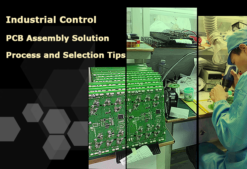
Prev:7 Key Reasons For Most Popular Artificial Intelligence Boost PCB Demand Products Today