
PCB via hole (Plated Through Hole, referred to as PTH) is a hole used on a printed circuit board (referred to as PCB), which is used for circuit paths between different layers on the PCB so that electronic components can be placed between multiple layers. Make electrical connections between them.

Large and small vias holes connect circuits board of different layers
The process of the via hole is to plate a layer of metal on the cylindrical surface of the via hole wall by chemical deposition to connect the copper foils that need to be connected in the middle layers, and the upper and lower sides of the via hole are made into ordinary pads. The shape can directly communicate with the lines on the upper and lower sides, or not. The via holes can be used for electrical connection, and the fixation increases the mechanical strength of the PCB, ensuring the correct installation and reliable connection of components.

Via hole technology on PCB board
PCB via types include standard through hole PTH (Plated Through Hole), blind hole (Blind Via) and buried hole (Buried Via)
Standard PTH connects different layers of the entire printing circuit board, which can be used to realize internal interconnection or as a component mounting positioning hole. Since the through hole is easier to recognize in the process and the cost is lower, the general printed circuit board uses the through-the-hole.
Refers to the top and bottom surface of the printed circuit board, with a certain depth, used for the connection of the surface circuit and the inner layer circuit below, and the depth and diameter of the hole usually do not exceed a specific ratio.
Refers to the connection hole located in the inner layer of the printed circuit board, which does not extend to the surface of the circuit board. Buried vias are inside the PCB and do not contact the surface.

PCB Plated Through-hole type: PTH、Blind Via、Buried Via
Use a drilling machine to drill holes in the PCB to form via holes. A high-speed drill is usually used, and its diameter depends on the required connection device and current requirements.
After drilling, the PCB needs to be cleaned to remove the swarf and residue from drilling.
In order to improve the conductivity and corrosion resistance of the inner wall of the via hole, the hole wall is usually chemically treated. This may involve using a chemical solution or electroplating to form a metal coating on the inside walls of the via.
Next, a metal layer is formed on the inner wall of the via through an electroplating process. The most common electroplating method is to deposit metal ions in the electrolyte on the inner walls of the vias by applying a current across the PCB.
After plating is complete, the PCB must be cleaned to remove any residual chemicals and surface treatment such as coating with preservatives or soldering media.
Through these steps, the vias on the PCB can be completed.

Steps of PCB Plated Through Holes
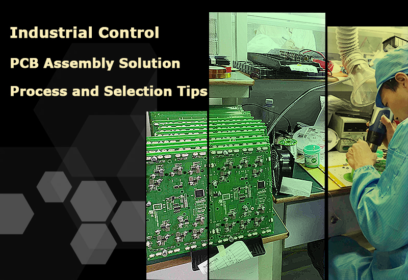
PCB plated through-hole design is an essential part of PCB design, and has a certain impact on signal integrity, especially high-speed signal lines. Therefore, a reasonable PCB via hole design is crucial to circuit performance, reliability, and manufacturing efficiency.
Prev:Capacitors Basic Guide: A Beginner's Manual for PCB Assembly Electronics Enthusiasts