HOME /Products /PCBA Services /PCB Assembly
☑ Equipped with advanced production equipment and automated production lines, efficient implementation of BGA patch assembly
☑ Technical support and services, providing customized solutions.
☑ The plant maintains a constant temperature and humidity environment to ensure the stability of assembly

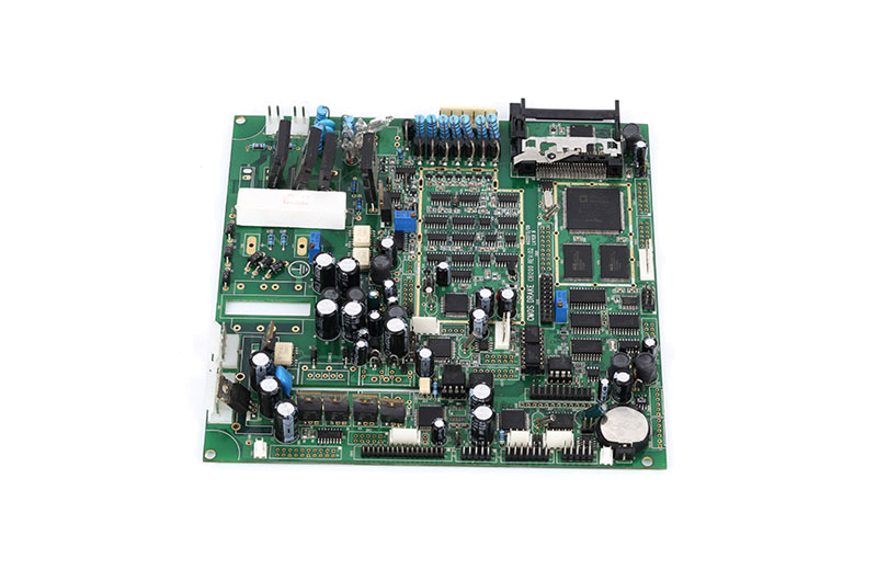
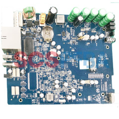
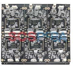
BGA (Ball Grid Array) technology in PCB assembly is a modern surface mount technology that is widely used in the field of electronic assembly.
The traditional DIP (Dual In-line Package) package has problems such as the limited number of pins and a large footprint, which cannot meet the growing demand for high-density packaging and high performance of electronic products. In order to overcome these problems, BGA technology for PCB assembly came into being.
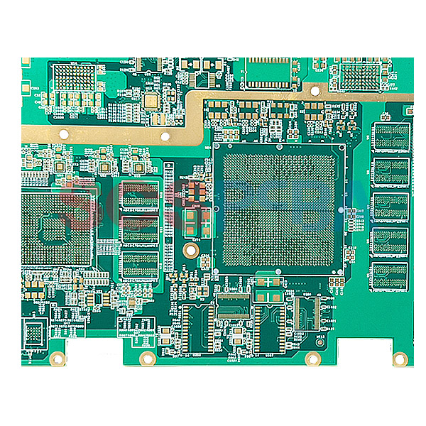
The importance of BGA technology is that it provides higher density and superior thermal performance for electronic assembly. In the BGA package, the pins of the chip are no longer directly exposed but are connected to the pads on the PCB (Printed Circuit Board) through a set of solder balls. Such a design makes the BGA chip have more pins, and the pin distribution is more uniform, which improves the density and performance of the PCB.
With the continuous development of electronic products towards miniaturization, lightweight, high performance and high reliability, BGA technology for PCB assembly has become more and more important. It is widely used in communication equipment, computer, industrial control and other fields. BGA technology provides effective solutions for high-speed transmission, high-density integrated circuits and large-scale integrated circuits.
SCSPCBA will take you to understand the BGA technology we use in the production of PCB assembly, including high-density packaging, excellent thermal performance and anti-cold burn concerns. It will also introduce the application of SCSPCBA using BGA technology in the fields of communication equipment, computer, industrial control, etc., as well as the key considerations in the manufacturing and repair stages. In-depth understanding of SCSPCBA's technical level in PCB assembly BGA, let us become your only reliable partner.

BGA technology allows more pins to be integrated in a smaller package. Compared with traditional DIP packages, the number of pins is higher, enabling more complex circuit designs in a limited space.
2. Excellent Thermal Performance
There is a set of solder balls under the BGA chip, which are used to connect with the corresponding pads on the PCB. This design enables the heat to be evenly distributed across the bottom of the chip, which is conducive to the use of high-power devices and improves the heat dissipation effect of the PCB.
3. Anti-cold Anxiety Concerns
Due to the uniform distribution of pins in the BGA package, there are fewer solder joints compared to traditional DIP-packages. Therefore, BGA packaging can reduce the occurrence of cold anxiety problems and improve the reliability of soldering.
4. High-performance Application
BGA technology is widely used in high-performance fields, such as communication equipment, computers, industrial control, etc. It can meet the needs of high-speed transmission and large-scale integrated circuits and is suitable for applications dealing with complex data and high-frequency signals.
5. Facilitate Automated Production
The structural characteristics of the BGA package make it easier to automate production. Using precise assembly equipment and technology, the soldering between chips and PCBs can be completed quickly and accurately.
6. Miniaturization and Lightweight
BGA technology makes the size of electronic assembly smaller, thereby realizing the miniaturization and light weight of electronic products, and is suitable for various portable devices.
7. High Reliability:
Since the solder joints are evenly distributed and the number of solder joints is reduced, the BGA package has high reliability and reduces failures caused by soldering problems.
8. Rich Application Fields:
BGA technology is not only suitable for communication equipment and computers but also widely used in automotive electronics, industrial control, medical equipment and other fields, covering a variety of application scenarios.

● Layout Design
During the PCB design process, it is necessary to reasonably layout the location of the BGA package and the pin connection to ensure sufficient spacing between the pins, and to avoid increased soldering difficulty due to excessive density.
● Thermal Management
Consider the thermal management of the BGA chip and choose an appropriate cooling solution to ensure that the operating temperature of the chip is within a safe range and avoid thermal damage and performance degradation.
● Pad Design
Design a reasonable pad shape and size to ensure that it corresponds to the ball array of the BGA package. Pads that are too small may result in weak soldering, while pads that are too large may result in inaccurate soldering.
● Accurate PCB Assembly Technology
The installation of BGA chips requires high-precision assembly equipment and technology to ensure the precise alignment of BGA ball arrays and PCB pads. Precise assembly technology is the key to ensuring welding quality.
● Precise Reflow Soldering
Reflow soldering is a key step in connecting BGA chips to PCB pads. Control the temperature profile and time of reflow soldering to ensure the best state of melting and alloying of chips and pads during soldering.
● Environmental Control
It is necessary to maintain a constant temperature and humidity environment during the manufacturing process to avoid moisture absorption of humidity-sensitive components and lead to soldering problems. Environmental control is critical to ensure solder quality and assembly stability.
● X-ray Inspection:
X-ray inspection technology is used to check the quality of BGA soldering to ensure that there are no soldering defects, such as virtual soldering, solder balls are not full and so on. X-ray inspection can help to detect potential problems early and improve the reliability of PCB assembly manufacturing.

Put BGA chips and SMD components on the designated position of the PCB board in the correct direction and position.
Apply an appropriate amount of solder glue on the PCB to fix the BGA chip and SMD components in the correct position.
Send the assembled PCB board into the reflow soldering equipment, by controlling the temperature curve and time, the solder glue and the pad are melted, and the BGA chip and SMD components are firmly soldered to the PCB board.

After the soldering is completed, take the PCB board out of the reflow soldering equipment and let it cool naturally.
Use tools such as X-ray inspection to inspect the soldering quality to ensure that there are no soldering defects, such as virtual soldering, solder balls are not full, etc.
Clean the PCB board after soldering to remove residual soldering glue and impurities.
Conduct functional testing and performance testing to ensure that the assembled PCB board can work properly.