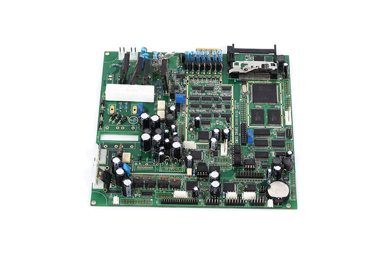
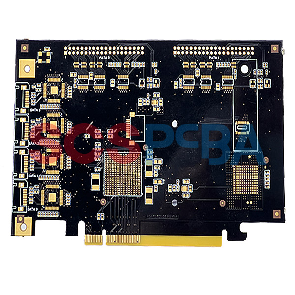
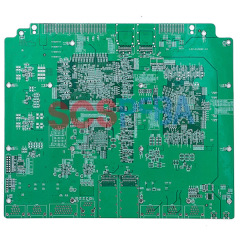
What Is HDI PCB
The HDI process is a high-density interconnection technology used to manufacture high-performance and high-density printed circuit boards (PCBs). HDI technology achieves more compact and complex circuit layouts by increasing the number of layers, reducing the line widths and spacing, and adopting advanced manufacturing processes.
The Main Features And Advantages of HDI Technology Include
1) Multilayer design: HDI technology utilizes multilayer circuit board design, which allows more circuit connections to be realized on a smaller area. By increasing the number of layers, the HDI technology provides higher wiring density and more complex circuit structures.
2) Smaller line widths and spacing: HDI technology uses smaller line widths and spacing, enabling more signal lines and power lines to be routed within limited space. This helps reduce circuit board size and weight while improving signal integrity and circuit performance.
3) Blind vias and buried vias: Blind and buried vias are widely used in the HDI process to reduce the length and delay of circuit paths and enhancing the speed and reliability of signal transmission. Blind vias and buried vias also help save space and provide greater design flexibility.
4) Microvia technology: HDI technology also includes microvia technology to achieve smaller vias size and higher connection density. Microvia technology commonly utilizes advanced techniques such as laser drilling or mechanical drilling to realize the manufacture of tiny holes.
5) High-speed signal transmission: Since the HDI technology provides shorter circuit paths and lower signal delays, it is suitable for high-speed signal transmission applications, such as high-speed communications, computer networks, and embedded systems.
The implementation of HDI technology requires advanced manufacturing technology and equipment, SCSPCBA can make HDI PCB with any layer interconnection. About the cost and technical details, please feel free to contact us.
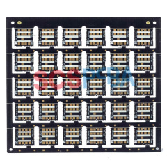
What Is Blind And Buried
Blind and buried vias are two types of vias commonly used in printed circuit board (PCB) designs to provide interconnections between different layers of the board.
Blind vias are vias that connected the outer layer to other inner layers, but they do not extend through the whole board. Blind vias allow for shorter interconnections, reducing signal delays and improving overall performance. They are commonly used when space is limited on the PCB outer layers, or when high-density components require shorter connections.
On the other hand, buried vias are vias that connected inner layers without extending to the outer layers. During the manufacturing process, the vias are drilled and filled with conductive material between the inner layers, without penetrating the outer layers. Buried vias can improve design flexibility and enable more complex multilayer PCB designs, as they free up space on the outer layers for routing traces or placing components.
The Following Parameters Need to be Considered When Designing A Circuit Board With Blind And Buried Vias:
1) Blind and buried vias' location
2) Blind and buried vias' number and size
3) The layers in which blind vias and buried vias are located
4) Blind and buried vias' specifications
5) PCB layer stack-up
6) Material and process requirements