Qingyuan Two-day and One-night Team-building Activity
Design for Manufacturability (DFM) is the practice of designing …
Design for Manufacturability (DFM) is the practice of designing …
Design for Manufacturability (DFM) is the practice of designing …
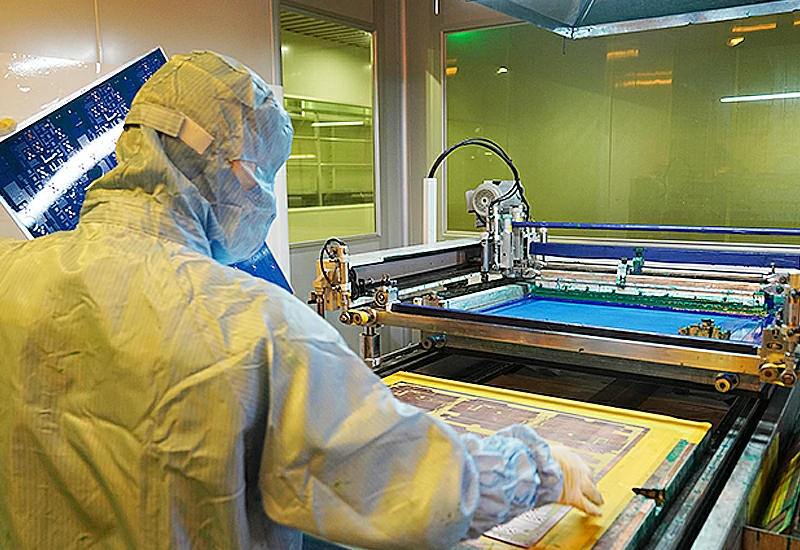
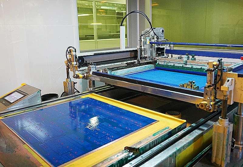
The solder mask should fully cover copper foil but reserve a 0.1–0.15mm retreat distance from pads to avoid covering them. This detail is especially critical for high-frequency PCBs, HDI PCB boards, or BGA packages, where solder mask thickness control directly impacts pad alignment and solderability.


https://www.scspcba.com/wp-content/uploads/2026/11/PCBA-Production-Workflow-What-Happens-from-Engineering-Review-to-Final-Delivery.webp
941
1672
administrator
https://scspcba.com/wp-content/uploads/2026/05/scspcba-home-logo.svg
administrator2026-11-12 11:08:012026-11-11 14:12:11PCBA Production Workflow: What Happens from Engineering Review to Final Delivery?
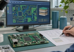
https://www.scspcba.com/wp-content/uploads/2026/11/How-PCB-Design-Decisions-Affect-PCBA-Manufacturing-Yield-Cost-and-Reliability.webp
941
1672
administrator
https://scspcba.com/wp-content/uploads/2026/05/scspcba-home-logo.svg
administrator2026-11-11 14:06:452026-11-11 14:07:29How PCB Design Decisions Affect PCBA Manufacturing Yield, Cost, and Reliability
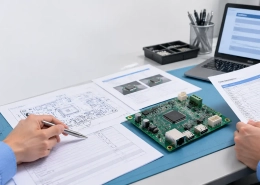
https://www.scspcba.com/wp-content/uploads/2026/11/OEM-PCBA-Manufacturing-Checklist.webp
941
1672
administrator
https://scspcba.com/wp-content/uploads/2026/05/scspcba-home-logo.svg
administrator2026-11-06 14:04:142026-11-11 14:08:53OEM PCBA Manufacturing Checklist: What to Confirm Before Mass Production
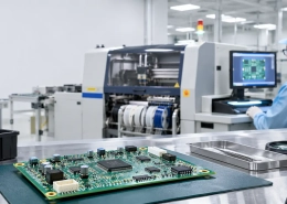
https://www.scspcba.com/wp-content/uploads/2026/11/How-Modern-EMS-Providers-Improve-PCBA-Manufacturing-Through-Automation-and-Quality-Control.webp
941
1672
administrator
https://scspcba.com/wp-content/uploads/2026/05/scspcba-home-logo.svg
administrator2026-11-06 14:02:112026-11-11 14:07:58How Modern EMS Providers Improve PCBA Manufacturing Through Automation and Quality Control
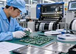
https://www.scspcba.com/wp-content/uploads/2026/10/Why-Small-Batch-PCBA-Costs-More-Per-Unit.webp
941
1672
administrator
https://scspcba.com/wp-content/uploads/2026/05/scspcba-home-logo.svg
administrator2026-10-30 13:27:102026-10-30 13:27:51Why Small-Batch PCBA Costs More Per Unit
Design for Manufacturability (DFM) is the practice of designing …
Design for Manufacturability (DFM) is the practice of designing …
In the modern electronic manufacturing industry, surface mounting technology ( SMT )has become an important circuit board assembly method and is widely used in smartphones, medical equipment, automotive electronics, industrial control, and other fields.
SMT production line consists of multiple key circuit board manufacturing process sections, each of which is crucial to the quality of the final product:
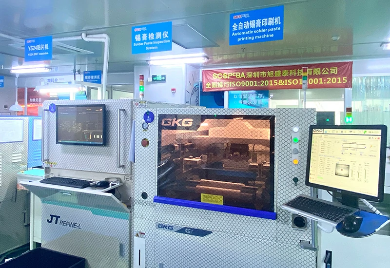
(1 ) Solder Paste Printer
(2) SPI Inspection
(3) High-speed/Multi-function Placement Machine
(4 ) Reflow Oven
(5 ) AOI Automatic Optical Inspection
(6 ) X-RAY Solder Joint Inspection
As a key material in SMT surface mount technology, solder paste is extremely sensitive to temperature and humidity. The PEMS Intelligent Solder Paste Cabinet provides a constant temperature and humidity environment to ensure that the solder paste is stored in an ideal state to avoid oxidation or decreased activity.
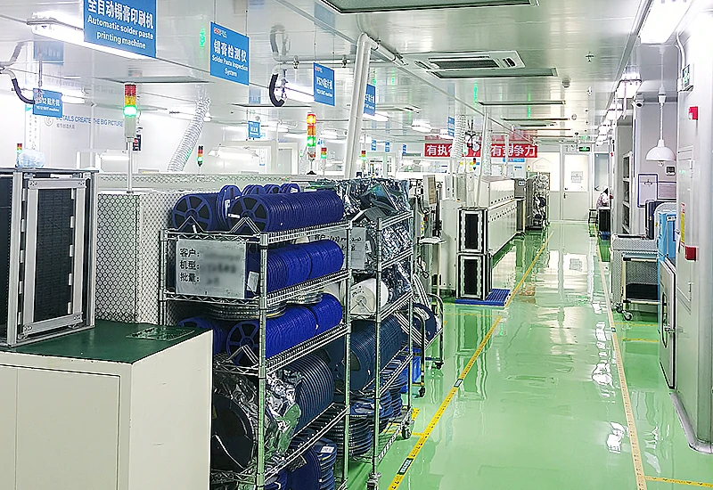
In the SMT production process, the quality management system plays a vital role, which is directly related to the yield and reliability of the circuit board. In order to ensure the welding quality and mounting accuracy, printed circuit board manufacturers generally introduce multi-level detection methods.
SPI (Solder Paste Detection), located after the printing process, detects key parameters such as solder paste thickness, height, and area, which can effectively prevent defects such as insufficient solder, solder bridges, and cold solder joints, laying a good foundation for subsequent surface mounting links.
AOI automatic optical inspection is performed after patching and reflow soldering. It uses high-definition cameras and image comparison technology to identify problems such as offset, reverse, missing, wrong and poor soldering. It has high accuracy and fast detection speed, which significantly improves the production efficiency and yield rate of board for circuit.
X-ray detection can see through the internal structure of solder joints and judge defects such as empty solder joints, solder ball offset, and missing pads. It is an indispensable detection method for high-end printed circuit board manufacturing.
Connect with the MES system to achieve full process data tracking from incoming materials to shipment. Each circuit board has its independent production history, including process parameters, test results, responsible persons and other information, to ensure that problems can be traced, quality can be controlled, and customers can rest assured.
SCSPCBA has the above set of strict quality control systems, which has built the trust foundation of SMT manufacturing and is the high reliability and consistency of printed circuit assembly.
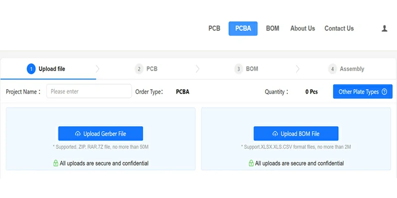
In the rapidly changing electronics manufacturing market, efficiency and transparency have become important criteria for customers to choose SMT suppliers. To this end, SCSPCBA circuit board manufacturers have developed an advanced online quotation system, dedicated to providing customers with fast, intelligent, accurate and transparent one-stop PCBA quotation services, greatly simplifying the procurement process and improving product launch speed.
Users only need to upload BOM and Gerber files, and the system can instantly analyze key information such as component model, package, usage and PCB board layer structure, and quickly estimate material costs. The system connects to multiple mainstream component supplier platforms, compares spot prices and batch inventory information in real time, and helps customers choose the most cost-effective device solution.
Through AI big data analysis, the system can also automatically recommend equivalent alternative components and select available solutions from a database of more than 10,000 products to further optimize the cost structure. In periods of component shortage or price fluctuations, multi-supplier price comparison and alternative suggestions are provided to keep customers in control.
The entire system can generate a full-process quotation including material procurement, PCB manufacturing, SMT patch, and functional testing within 10 seconds, and clearly list the details of each cost. The price is transparent and there is no hidden cost, which greatly enhances customer trust.
Customers can place orders with one click and track the entire process of production orders through the system, including key links such as material completeness, patch progress, test nodes, and delivery time, truly realizing a digital and visual project management experience.
SCSPCBA PCB board manufacturers has created a closed loop of intelligent manufacturing that integrates component procurement, PCB manufacturing, SMT assembly, functional testing, and finished product assembly, thereby achieving:
Whether it is a start-up technology company or an international brand, choosing an experienced, advanced equipment, and a sound quality system SMT supplier is a key step in the successful launch of a product.
If you are looking for a trustworthy SMT partner, welcome to experience our 10-second intelligent quotation system, or visit our SMT smart factory to experience the charm of “efficiency + quality” in smart manufacturing.
https://www.scspcba.com/wp-content/uploads/2026/11/PCBA-Production-Workflow-What-Happens-from-Engineering-Review-to-Final-Delivery.webp
941
1672
administrator
https://scspcba.com/wp-content/uploads/2026/05/scspcba-home-logo.svg
administrator2026-11-12 11:08:012026-11-11 14:12:11PCBA Production Workflow: What Happens from Engineering Review to Final Delivery?
https://www.scspcba.com/wp-content/uploads/2026/11/How-PCB-Design-Decisions-Affect-PCBA-Manufacturing-Yield-Cost-and-Reliability.webp
941
1672
administrator
https://scspcba.com/wp-content/uploads/2026/05/scspcba-home-logo.svg
administrator2026-11-11 14:06:452026-11-11 14:07:29How PCB Design Decisions Affect PCBA Manufacturing Yield, Cost, and Reliability
https://www.scspcba.com/wp-content/uploads/2026/11/OEM-PCBA-Manufacturing-Checklist.webp
941
1672
administrator
https://scspcba.com/wp-content/uploads/2026/05/scspcba-home-logo.svg
administrator2026-11-06 14:04:142026-11-11 14:08:53OEM PCBA Manufacturing Checklist: What to Confirm Before Mass Production
https://www.scspcba.com/wp-content/uploads/2026/11/How-Modern-EMS-Providers-Improve-PCBA-Manufacturing-Through-Automation-and-Quality-Control.webp
941
1672
administrator
https://scspcba.com/wp-content/uploads/2026/05/scspcba-home-logo.svg
administrator2026-11-06 14:02:112026-11-11 14:07:58How Modern EMS Providers Improve PCBA Manufacturing Through Automation and Quality Control
https://www.scspcba.com/wp-content/uploads/2026/10/Why-Small-Batch-PCBA-Costs-More-Per-Unit.webp
941
1672
administrator
https://scspcba.com/wp-content/uploads/2026/05/scspcba-home-logo.svg
administrator2026-10-30 13:27:102026-10-30 13:27:51Why Small-Batch PCBA Costs More Per Unit
Design for Manufacturability (DFM) is the practice of designing …
Design for Manufacturability (DFM) is the practice of designing …
Design for Manufacturability (DFM) is the practice of designing …
Box Build Assembly has become an important bridge between electronic design and final products in modern electronic manufacturing. The perfect integration of circuit boards and structural parts determines product performance and affects delivery speed and market competitiveness.
1. What is Box Build Assembly?
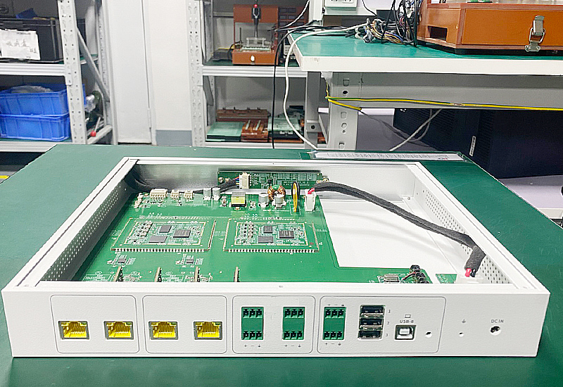
Box Build Assembly, also known as system integration or complete machine assembly, refers to integrating multiple electronic, electrical and mechanical components into a complete package. It goes beyond traditional PCB assembly and covers housing installation, cable connection, functional module integration and final testing. It is one of the most complex and closest links to the final product in electronic manufacturing services (EMS).
Box Build Assembly usually includes the following key components:
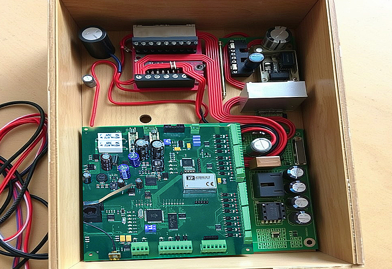
In box build assembly process, circuit board manufacturing is the “nerve center” of the whole system. We have mature DIP and SMT mounting technologies in PCB integrated circuit solution, supporting complex requirements from Double Layer PCB, Multilayer PCB, HDI PCB, Aluminum PCB, Ceramic PCB, Thick Copper PCB, High-Tg PCB to mixed assembly.
Integrated capabilities from circuit design, electronic components procurement, PCB board fabrication, printed circuit assembly, surface mounting technology, plug-in, structural parts customization, to whole machine testing.
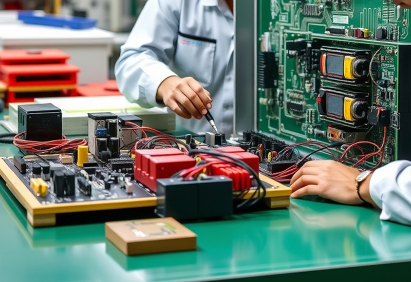
Box build assembly manufacturing is widely used in the following industries:
| Industries | application |
|---|---|
| Industrial Control | Power control box, Instrument housing |
| Medical Electronics | Wearable health equipment, Detector housing system |
| Communications | Router, Antenna box, 5G base station submodule |
| Smart Home | Smart gateway, Central control system, Security terminal |
| Automotive Electronics | In-vehicle controller, Charging pile main control box |
| Consumer Electronics | Audio system, Smart wearable host |
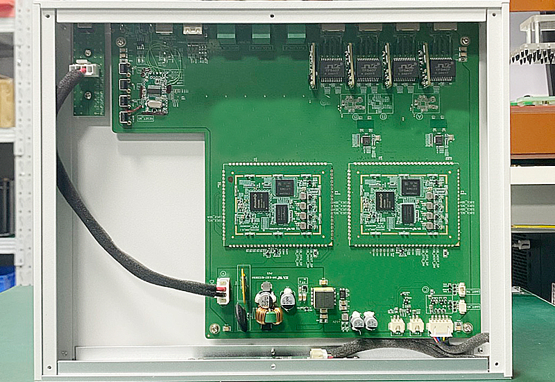
SCSPCBA printed circuit board manufacturer, adopts a standardized and flexible whole-machine assembly process to ensure product stability and consistency:
– Analyze customer drawings, optimize PCB design, and confirm the feasibility of printed circuit assembly
– Carry out full-process electronic components procurement and warehouse material preparation according to the customer BOM
– SMT surface mount technology, AOI/X-ray inspection, functional testing
– Homemade wiring harnesses, plastic parts, metal brackets and other parts
– Combining manual and automated processes to complete multi-step system integration
– Functional testing, aging testing, waterproofing/drop testing
– Customized packaging, anti-static/shockproof treatment
https://www.scspcba.com/wp-content/uploads/2026/11/PCBA-Production-Workflow-What-Happens-from-Engineering-Review-to-Final-Delivery.webp
941
1672
administrator
https://scspcba.com/wp-content/uploads/2026/05/scspcba-home-logo.svg
administrator2026-11-12 11:08:012026-11-11 14:12:11PCBA Production Workflow: What Happens from Engineering Review to Final Delivery?
https://www.scspcba.com/wp-content/uploads/2026/11/How-PCB-Design-Decisions-Affect-PCBA-Manufacturing-Yield-Cost-and-Reliability.webp
941
1672
administrator
https://scspcba.com/wp-content/uploads/2026/05/scspcba-home-logo.svg
administrator2026-11-11 14:06:452026-11-11 14:07:29How PCB Design Decisions Affect PCBA Manufacturing Yield, Cost, and Reliability
https://www.scspcba.com/wp-content/uploads/2026/11/OEM-PCBA-Manufacturing-Checklist.webp
941
1672
administrator
https://scspcba.com/wp-content/uploads/2026/05/scspcba-home-logo.svg
administrator2026-11-06 14:04:142026-11-11 14:08:53OEM PCBA Manufacturing Checklist: What to Confirm Before Mass Production
https://www.scspcba.com/wp-content/uploads/2026/11/How-Modern-EMS-Providers-Improve-PCBA-Manufacturing-Through-Automation-and-Quality-Control.webp
941
1672
administrator
https://scspcba.com/wp-content/uploads/2026/05/scspcba-home-logo.svg
administrator2026-11-06 14:02:112026-11-11 14:07:58How Modern EMS Providers Improve PCBA Manufacturing Through Automation and Quality Control
https://www.scspcba.com/wp-content/uploads/2026/10/Why-Small-Batch-PCBA-Costs-More-Per-Unit.webp
941
1672
administrator
https://scspcba.com/wp-content/uploads/2026/05/scspcba-home-logo.svg
administrator2026-10-30 13:27:102026-10-30 13:27:51Why Small-Batch PCBA Costs More Per Unit