Industrial Control PCB Assembly: High Reliability and Cost Efficiency
Design for Manufacturability (DFM) is the practice of designing …
Design for Manufacturability (DFM) is the practice of designing …
Design for Manufacturability (DFM) is the practice of designing …
Design for Manufacturability (DFM) is the practice of designing …
PCBA Functional Test (FCT) is a testing process for overall functional verification of the one-stop printed circuit board assembly manufacturing. It aims to simulate the actual working environment and ensure the integrity and reliability of the collaborative work of software and hardware.
In modern electronic manufacturing, PCBA functional testing (FCT) represents the final and most critical stage of the quality assurance process. It is not just a simple pass/fail inspection, but a comprehensive evaluation that determines whether the assembled board can reliably deliver its intended performance in real-world applications.
Functional testing validates whether the PCBA design performs as expected across its core operating domains—including power management, signal processing, data communication, and user interface control.
This step ensures that the design intent translates accurately into real functionality, confirming that hardware and embedded software operate harmoniously within system specifications.
Even after advanced SMT circuit board and optical inspections, hidden manufacturing defects may remain—such as cold solder joints, misplaced components, or incorrect component values.
Through FCT, these latent faults can be identified under simulated working conditions, preventing defective circuit boards from reaching the customer.
When integrated with In-Circuit Testing (ICT) earlier in the circuit board manufacturing process, it forms a dual defense mechanism: ICT isolates component-level issues, while FCT validates system-level functionality.
A truly reliable printed circuit assembly must sustain performance across varying temperatures, humidity, and vibration environments.
Functional testing often incorporates environmental stress simulation, ensuring that circuits maintain stability under real-life conditions such as high-temperature operation or mechanical vibration.
This not only improves circuit on board durability but also provides predictive insights into long-term reliability and lifecycle performance.
PCB fabrication and assembly testing is not limited to a single point in production; it evolves alongside the product lifecycle. Both In-Circuit Testing (ICT) and Functional Circuit Testing (FCT) play critical roles across different stages—from early prototyping to post-repair validation.
At the early design stage, FCT takes the lead. Engineers perform first-version PCB board sample testing to verify the functionality of critical modules, such as the main controller, power circuitry, and signal interfaces.
This ensures that the PCB layout, firmware, and system logic meet design expectations before moving into pilot production.
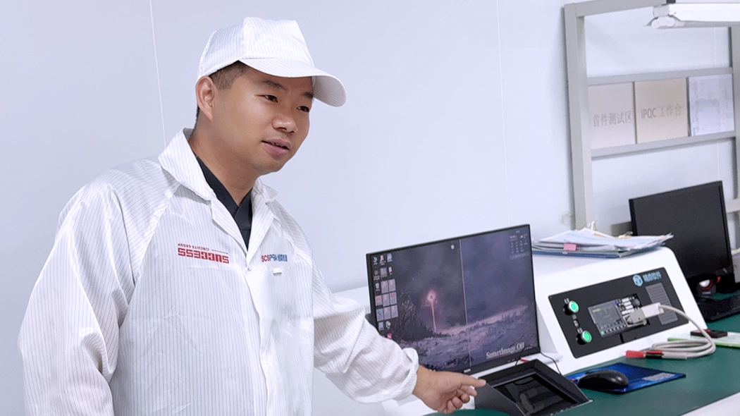
During volume PCB board fabrication, both ICT and FCT are used in tandem.
This dual-layer testing ensures that every PCBA leaving the production line complies with factory acceptance standards, improving the overall first-pass yield and reducing post-delivery failures.
After a defective PCBA circuit board is reworked or repaired, a secondary round of ICT and FCT is essential.
By standardizing these testing phases across the PCB manufacturing assembly lifecycle, printed circuit board assembly manufacturers can establish a closed-loop quality system, ensuring consistent reliability from PCB prototype to production to after-sales service.
| Category | FCT (Functional Circuit Test) | ICT (In-Circuit Test) |
|---|---|---|
| Purpose | Validates system-level functionality under real conditions | Checks electrical connections and components parts individually |
| Testing Stage | After full PCBA assembly | After SMT or THT stage |
| Test Content | Software logic, signal response, power output, interface communication | Shorts, opens, resistors, capacitors, diode polarity, etc. |
| Advantages | Simulates real operation, ensures system performance | High precision fault localization, early defect screening |
| Limitations | Requires custom fixture and firmware, slower | Cannot verify system-level logic or firmware behavior |
For high-reliability applications such as automotive control modules, medical devices, and power management systems, combining ICT + FCT forms a double-layer quality defense, ensuring both component-level and system-level reliability.
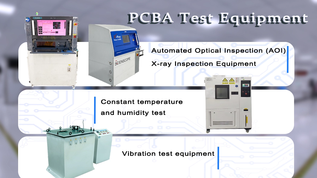
PCBA manufacturing testing equipment uses electrical, welding, and environmental reliability methods to detect solder joint quality, environmental adaptability, and functional reliability. Typical equipment is as follows:
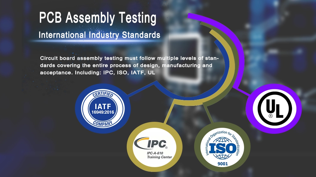
Circuit board assembly testing must follow multi-level standards, covering the entire process of design, manufacturing, and acceptance. The core standards are as follows:
Scope: Globally recognized standard for assessing the appearance and solder quality of printed circuit board assembly manufacturing.
Key Contents:
Scope of application: Electrical connectivity testing of PCBs and PCBAs (ICT testing phase).
Key points:
Scope: Specifies physical, chemical, and electrical test methods for PCB board fabrication or printed circuit board assembly.
Key Contents:
Scope of Application: General quality system framework, ensuring traceability and consistency from design to shipment.
Application in PCB assembly services:
Scope of Application: Quality management standards for automotive electronics products (including automotive PCBAs).
Texting Content:
Scope of application: Medical electronic PCBA manufacturing.
Texting Content:
Scope: Electrical safety and fire protection standards.
Texting Content:
(1) False Solder Joints
(1) Component Damage
(2) Reverse Polarity
(1) Short Circuit
(2) Open Circuit
(1) Moisture/Contamination
(2) EMI Interference
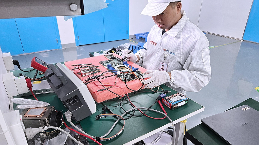
During a batch test of automotive pcb assembly and manufacturing control boards, the initial pass rate reached 99%. However, after delivery, customers reported frequent Wi-Fi disconnections in high-temperature environments. Repair analysis pointed to communication anomalies with the main control chip, but routine functional testing revealed no faults.
Engineers used a customized PCBA test rig to simulate high-temperature cycling tests. When the ambient temperature rose to 65°C, the test rig detected abnormal impedance fluctuations in the MLCC capacitor (number C107) adjacent to the main control chip. Disassembly revealed the following:
Without FCT testing, this potential risk could cause a power outage or control failure during vehicle operation.
Through statistical analysis and traceability of failure data, the production line promptly optimized the reflow soldering temperature profile and placement pressure settings, increasing the yield from 98.3% to 99.8% while also reducing customer returns.
An efficient PCBA testing process typically includes the following steps:
Through digital test data management and automated inspection systems, PCB assembly manufacturers can:
With increasingly fierce competition in the smart manufacturing and electronics industries, printed circuit assembly functional testing is no longer an option but a strategic core for quality assurance.
From ICT to FCT to reliability verification, every step safeguards final product performance.
Only through a scientific, systematic, and standardized testing system can companies achieve the optimal balance between shipment volume and quality, earning market trust and long-term partnerships.

-36x36.png)


https://www.scspcba.com/wp-content/uploads/2026/10/SCSPCBA-October-2026-Update_featured.webp
619
724
administrator
https://scspcba.com/wp-content/uploads/2026/05/scspcba-home-logo.svg
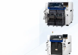
administrator2026-10-16 11:50:002026-10-19 13:22:36SCSPCBA October 2026 Update: SMT Equipment Upgrades, Flying Probe Testing and Online Ordering
https://www.scspcba.com/wp-content/uploads/2026/10/How-to-Reduce-PCBA-Cost-Without-Sacrificing-Quality-Proven-Guide_featured.webp
308
554
administrator
https://scspcba.com/wp-content/uploads/2026/05/scspcba-home-logo.svg
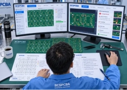
administrator2026-10-15 18:00:002026-10-19 13:20:29How to Reduce PCBA Cost Without Reducing Quality
https://www.scspcba.com/wp-content/uploads/2026/09/Applications-of-PCBA-in-Modern-Electronics.webp
311
554
administrator
https://scspcba.com/wp-content/uploads/2026/05/scspcba-home-logo.svg
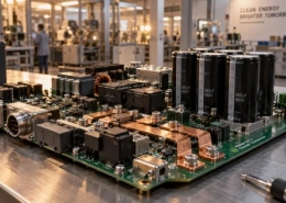
administrator2026-10-09 00:00:222026-09-29 02:02:53Applications of PCBA in Modern Electronics
https://www.scspcba.com/wp-content/uploads/2026/09/How-Reflow-Soldering-Affects-PCBA-Quality.webp
310
553
administrator
https://scspcba.com/wp-content/uploads/2026/05/scspcba-home-logo.svg
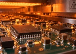
administrator2026-10-02 00:00:192026-09-29 02:02:29How Reflow Soldering Affects PCBA Quality

https://www.scspcba.com/wp-content/uploads/2026/09/Who-Is-the-Manufacturer-of-PCB-Board-in-China.webp
307
554
administrator
https://scspcba.com/wp-content/uploads/2026/05/scspcba-home-logo.svg
administrator2026-09-25 00:00:162026-09-28 02:17:09Who Is the Manufacturer of PCB Board in China?
Design for Manufacturability (DFM) is the practice of designing …
Design for Manufacturability (DFM) is the practice of designing …
From October 8–11, 2025, the MOBISAD IMEX electronics exhibition in Istanbul will gather global leaders in electronics manufacturing, mobile technology, and PCB assembly solutions. For visitors, this event is not just another trade fair—it is an opportunity to experience groundbreaking PCB manufacturing, PCBA Turkey solutions, and future-ready electronics innovations all under one roof.
At MOBISAD IMEX 2025, exhibitors such as SCSPCBA will present the complete printed circuit board fabrication process, from multi-layer PCB boards to high-density interconnect (HDI) solutions. For those looking for a PCB manufacturer in Turkey, this exhibition offers the perfect opportunity to compare advanced manufacturing capabilities and evaluate new suppliers. These technologies are reshaping applications in automotive electronics, medical devices, and consumer electronics.
Visitors will enjoy live showcases of SMT assembly and PCB assembly and manufacturing production. These demonstrations highlight both speed and precision in electronics manufacturing. For companies sourcing turnkey PCB assembly in Turkey, the live production lines provide a direct look at how prototypes evolve into fully assembled, reliable circuit boards.
From PCB prototyping to large-scale PCB board production, exhibitors will demonstrate how integrated solutions are supporting industries such as automotive, IoT, and industrial controls. With increasing demand across Europe and the Middle East, PCBA Turkey providers are positioning themselves as reliable partners for global buyers.
Beyond technology displays, visitors will also experience how PCB quote and PCBA online instant quotation platforms are transforming the way businesses manage procurement. Instead of waiting days for manual estimates, buyers can now access real-time PCB board pricing and PCBA assembly quotations directly at the SCSPCBA exhibition booths. This not only speeds up project planning but also ensures transparency and accuracy in circuit board manufacturing cost control—an innovation that many engineers and supply chain managers will find especially valuable.
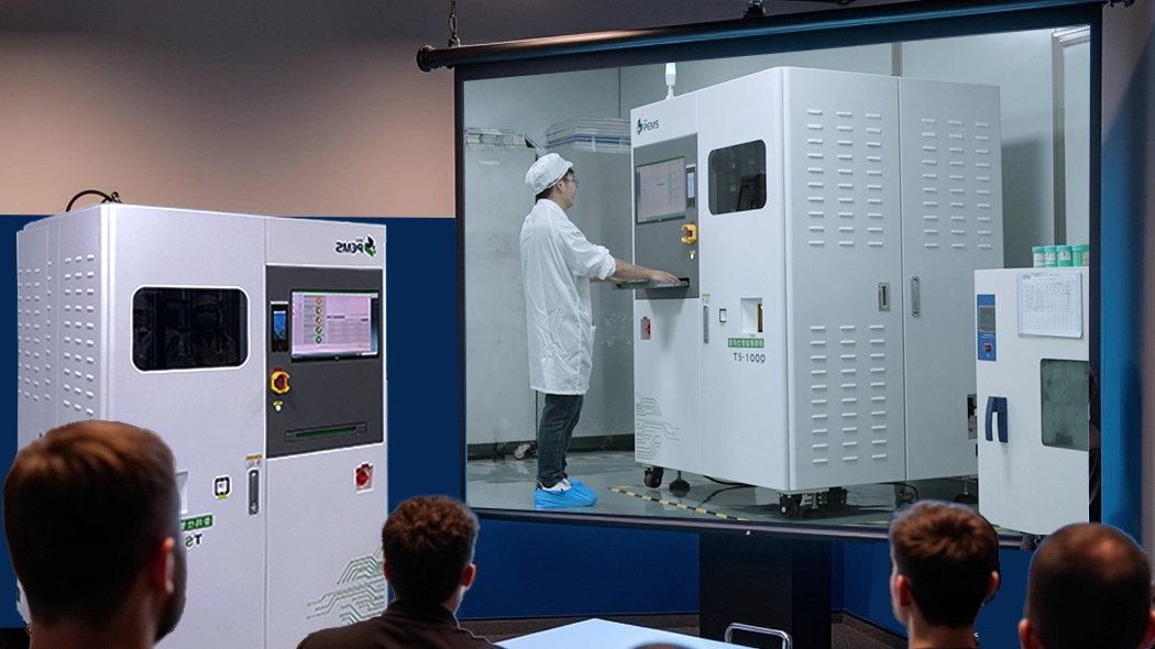
Istanbul is a strategic gateway between Europe and the Middle East, making it an attractive hub for electronics manufacturing Turkey. The city’s growing reputation as a destination for PCB and PCBA services gives international buyers confidence in sourcing locally while still benefiting from global-quality standards.
By meeting printed circuit board assembly manufacturers in Turkey at MOBISAD IMEX 2025, visitors can establish regional supply chains that reduce shipping costs, shorten lead times, and improve communication efficiency. For OEMs and startups alike, this regional advantage makes Istanbul a must-watch center for the future of electronics.
As you plan your visit to MOBISAD IMEX 2025, we at SCSPCBA invite you to make our booth a key stop on your exhibition journey. Here are a few tips to maximize your experience:
SCSPCBA will be located at booth 8A-157, within the PCB & PCBA innovation zones. Mark it on your exhibition guide to ensure you don’t miss it when exploring key areas of the electronics trade fair in Turkey.
Our team of engineers and procurement specialists will be available to discuss solutions ranging from automotive PCB assembly to turnkey PCB assembly Turkey projects. Visitors are encouraged to share their specific challenges and learn how SCSPCBA’s expertise can address them.
Take advantage of SCSPCBA’s instant PCB & PCBA quotation platform to see how your projects can move from idea to production faster. This hands-on demo will show you how to estimate costs with accuracy and confidence.
Whether you are searching for a PCB board fabrication Turkey, exploring printed circuit board assembly Turkey providers, or considering electronics manufacturing Istanbul for future projects, our booth is the right place to get practical, tailored advice.
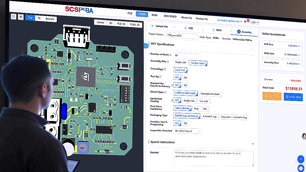
MOBISAD IMEX 2025 is set to be a hub of technological advancement, and the PCB manufacturing & PCB board assembly innovation zones are must-visit areas for any attendee. Whether you are exploring advanced PCB board fabrication, discovering new surface mounting technology assembly processes, or looking for one-stop electronics solutions, this exhibition offers valuable insights and hands-on experiences you simply can’t miss.
MOBISAD IMEX 2025 is shaping up to be the premier PCBA trade fair 2025 for Europe and the Middle East. For visitors, it’s the perfect chance to evaluate electronics manufacturing in Istanbul, connect with pcb manufacturers in Turkey, and explore turnkey PCB assembly Turkey solutions.
If you’re looking for innovation, efficiency, and reliability in PCB & PCBA services, make sure to visit SCSPCBA’s exhibition booth at MOBISAD IMEX 2025—a must-stop for forward-thinking businesses.
https://www.scspcba.com/wp-content/uploads/2026/10/SCSPCBA-October-2026-Update_featured.webp
619
724
administrator
https://scspcba.com/wp-content/uploads/2026/05/scspcba-home-logo.svg
administrator2026-10-16 11:50:002026-10-19 13:22:36SCSPCBA October 2026 Update: SMT Equipment Upgrades, Flying Probe Testing and Online Ordering
https://www.scspcba.com/wp-content/uploads/2026/10/How-to-Reduce-PCBA-Cost-Without-Sacrificing-Quality-Proven-Guide_featured.webp
308
554
administrator
https://scspcba.com/wp-content/uploads/2026/05/scspcba-home-logo.svg
administrator2026-10-15 18:00:002026-10-19 13:20:29How to Reduce PCBA Cost Without Reducing Quality
https://www.scspcba.com/wp-content/uploads/2026/09/Applications-of-PCBA-in-Modern-Electronics.webp
311
554
administrator
https://scspcba.com/wp-content/uploads/2026/05/scspcba-home-logo.svg
administrator2026-10-09 00:00:222026-09-29 02:02:53Applications of PCBA in Modern Electronics
https://www.scspcba.com/wp-content/uploads/2026/09/How-Reflow-Soldering-Affects-PCBA-Quality.webp
310
553
administrator
https://scspcba.com/wp-content/uploads/2026/05/scspcba-home-logo.svg
administrator2026-10-02 00:00:192026-09-29 02:02:29How Reflow Soldering Affects PCBA Quality
https://www.scspcba.com/wp-content/uploads/2026/09/Who-Is-the-Manufacturer-of-PCB-Board-in-China.webp
307
554
administrator
https://scspcba.com/wp-content/uploads/2026/05/scspcba-home-logo.svg
administrator2026-09-25 00:00:162026-09-28 02:17:09Who Is the Manufacturer of PCB Board in China?
Design for Manufacturability (DFM) is the practice of designing …
Design for Manufacturability (DFM) is the practice of designing …
Design for Manufacturability (DFM) is the practice of designing …