The inner layer pattern of PCB refers to the copper layer pattern located inside the PCB board and is used to connect different circuit components. The layout and design of these inner layer graphics directly affect the performance, functionality, reliability and cost of electronic devices.
The layout and connection method of the inner layer graphics determines the signal transmission speed and stability of the circuit. Such as chips, resistors, capacitors and various connectors, all need to be connected through inner graphics to form a complete circuit. Reasonable layout can reduce signal transmission delay and interference, and improve the transmission speed and stability of the PCB.
Reasonable inner-layer graphic design can improve the reliability of electronic products, reduce electromagnetic interference between circuit components, and improve the anti-interference ability of the circuit, thereby enhancing the reliability and stability of the equipment.
Reasonable layout and design can reduce the complexity and cost of the PCB board manufacturing process and can achieve a high degree of integration of circuits, allowing more electronic components and connection lines to be accommodated in a limited physical space. This is crucial for the design of miniaturized and lightweight electronic products, such as smartphones, tablets, etc., to improve production efficiency and thereby reduce the manufacturing cost of the product.
In the printed circuit board manufacturing process, automatic cutting (sheet material) is an important process. When selecting PCB materials, many factors need to be considered, such as electrical properties, thermal properties, mechanical strength and process requirements.
Cutting with an automatic cutting machine ensures the precise size and shape of the PCB. These machines are capable of highly accurate cutting through digital design and precision cutting technology. The use of automatic cutting machines can automatically arrange and optimize cutting plans based on design files to ensure optimal utilization of PCB materials, minimize material waste, reduce costs, improve production efficiency, and reduce the risk of human errors.
 steps")
PCB inner layer graphics-automatic cutting (sheet material) steps
During the PCB fabrication process, if dirt is present on the surface, it will affect the adhesion of the circuit board to other components, leading to poor welding and electrical connection problems. In addition, dirt may also cause circuit short circuits and instability, affecting the normal operation of the entire circuit system.
The PCB inner layer cleaning process is usually divided into several steps.
First, a solvent is needed to dissolve and remove oil, solder residue, and other impurities from the PCB surface. Commonly used solvents include alcohol, deionized water, and organic solvents. Choosing the appropriate solvent depends on the type of dirt on the PCB surface and cleaning requirements.
Secondly, cleaning equipment is also very important. Common cleaning equipment includes ultrasonic cleaning machines and spray cleaning machines. Ultrasonic cleaning machines use high-frequency vibrations of ultrasonic waves to clean the PCB surface, which can effectively remove tiny dirt. The spray cleaning machine sprays the cleaning liquid evenly on the PCB surface through the spray nozzle to achieve a thorough cleaning effect.
By cleaning the inner layer, you can ensure that the PCB surface is clean and flat, improve the adhesion performance of the circuit board, reduce manufacturing defects, and improve product quality.

PCB inner layer graphics cleaning steps
Laminating is the process of attaching a film to the inner graphics of the PCB. The film can provide an insulating layer between the inner graphics of the PCB to prevent short circuits between circuits. This is very important to ensure proper operation of the board, especially when the board has a complex circuit layout.
When selecting membrane materials, the special requirements of the circuit board need to be considered, such as operating temperature range, chemical environment, and mechanical strength. Make sure to choose high-quality membrane materials that meet the requirements to provide maximum insulation and protection, ensuring the reliability and stability of the circuit board.

PCB inner layer pattern film lamination process
Exposure is a process that uses photosensitive materials and lasers to create patterns on the inner layers of PCBs. The role of the laser is to achieve accurate exposure by controlling the intensity and position of the light. The correct setting of exposure parameters is very important to obtain high-quality PCB inner layer graphics.
During the exposure process, photosensitive film or photosensitive paint is placed on the PCB and then illuminated with a laser beam. The laser beam projects the graphics on the PCB onto the photosensitive material by controlling the exposure time and intensity. Photosensitive materials react chemically to form visible patterns when exposed to laser light.
The importance of exposure parameters cannot be ignored. These parameters include laser power, exposure time, and spot size. The laser power determines the intensity of the light, the exposure time determines the duration of the light, and the spot size determines the resolution of the pattern. Properly setting these parameters ensures exposure accuracy and consistency, resulting in high-quality PCB inner layer graphics.

PCB inner layers exposure process
Etching is a key step in the PCB inner layer pattern production process. It can ensure that only the required copper foil area is retained, thereby achieving the accuracy and integrity of circuit connections.
The following are the steps for etching:
· After exposure, the part of the photosensitive material not exposed to light is removed through chemical methods to expose the areas of the copper foil that need to be etched.
· Place the PCB into an etching bath containing etching fluid. The etching solution is usually an acidic solution such as copper chloride.
· The etching solution will react with the copper foil exposed to light, gradually corroding it away. This process takes a certain amount of time, and the specific time depends on the concentration of the etching solution and the etching depth requirements.
· When the required etching depth is reached, remove the PCB from the etching tank and clean it to remove residual etching liquid and photosensitive materials.

PCB inner layer pattern etching process
AOI inspection is a method that uses automated optical inspection technology to inspect the inner layer graphics of PCB. It uses high-resolution cameras and image-processing algorithms to scan PCBs and detect possible defects and errors.
During the AOI inspection, the camera scans each area on the PCB and transmits the images to the image processing system for analysis. Image processing algorithms will detect possible defects and errors, such as welding problems, component position deviations, short circuits, open circuits, etc., based on preset rules and standards.
AOI inspection can efficiently detect defects and errors in PCB inner layer graphics, with higher accuracy and speed than manual inspection. It can quickly scan the entire PCB and provide accurate detection results in a short time. In addition, AOI inspection can also reduce the possibility of manual errors and increase production efficiency.
PCB inner layer pattern AOI inspection
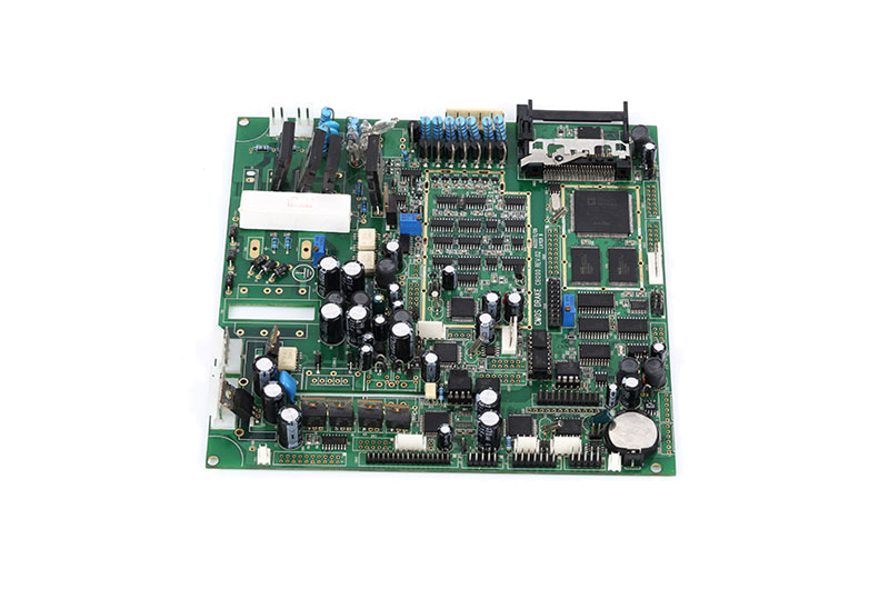
PCB inner-layer graphics are widely used in different fields, and their importance cannot be ignored. PCB inner layer graphics, especially in the field of industrial control, provide stable and reliable circuit connection and control functions for industrial control equipment, industrial control systems and various industrial control applications.
Industrial control equipment usually needs to process large amounts of data and signals, so it requires more electronic components and connecting lines. Inner layer graphics allow routing on the PCB to become more compact and dense, thereby reducing the size of the PCB while increasing its functionality. Such as PLC (programmable logic controller), DCS (distributed control system), HMI (human-machine interface), etc. These devices often require highly reliable circuit boards to ensure stable operation.
Industrial control systems have extremely high requirements for signal accuracy and stability. The design and manufacturing of PCB inner layer graphics can help industrial control systems meet the high requirements for signal accuracy and stability, reduce signal interference and crosstalk, and thus ensure the quality of signal transmission on the PCB. For example, it is used to connect various control components, sensors, actuators, and controllers to improve the performance and reliability of industrial control systems through reasonable layout and design.
PCB inner layer graphics are also widely used in other applications in the field of industrial control. Examples include industrial furnaces, cooling systems and chemical processing units. These applications require precise circuit design and reliable manufacturing to ensure proper operation and safety of the device.
上一条:Let You Understand The PCB Lamination Process In 3 Minutes
下一条:The Process of Multi-layer PCB Fabrication And Application In Industrial Control