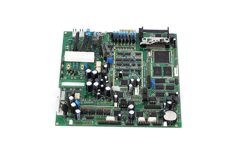
Printed circuit board Pad design is one of the primary factors affecting pad quality. Reasonable pad design can improve the reliable connection between the pad and components and effectively avoid welding defects.
Poor Pad Design Includes:The component type and size are not selected, and there is a lack of effective contact area and connection strength between the pad and the component.
The spacing between the solder pads and the circuit board and the narrow design space of the via holes, leading to problems such as short circuits or open solder pads.
There is no trimming at the corners of the soldering pad, which will affect the installation and welding of the plug-in.
Pad Design Flaws Solution: Improve pad design and select pad size to match component type and size. Depending on the size and arrangement of components, select appropriately sized and shaped pads to ensure adequate contact area and connection strength. Also, optimize the component layout to ensure sufficient space between the pads and the circuit board. Making the edges of the pads smoother by removing sharp corners or applying appropriate fillets helps align the plug-in and smooth the soldering process.

Welding manufacturing is critical to the control of pad quality. Rigorous soldering manufacturing processes ensure high-quality soldering connections between pads and components, improving printed circuit boards quality.
Poorly Manufactured Pads Include:
During the welding process, incompletely melted solder or other impurities may lead to the generation of dross at the welding point.
Solution: Increase the viscosity of the solder paste, adjust the heating temperature and time, and clean the welding equipment regularly.
During the welding process, if there is a conductive substance between two different solder joints, it may cause a short circuit.
Solution: Strengthen quality inspection to ensure insulation between solder joints.
Improper parameters during welding, uneven shape or distribution of solder balls, may lead to problems such as poor welding, short circuit or virtual soldering of pads.
Solution: Adjust welding parameters such as temperature, time and pressure to ensure that the solder balls can be evenly coated on the pads and welded components, thereby reducing the risk of welding defects.
The adhesion between the pad and the substrate is insufficient, causing the connection between the pad and the wire to loosen or fall off.
Solution: Before soldering, make sure the pad and wire surfaces are clean to remove oxides and dirt to promote solder adhesion to the substrate. Moderately increase the amount of solder to ensure that the solder fully wets the pads and wires and improves the soldering contact area and adhesion.
The solder paste overflows the pad during the patch welding process, which may cause short circuit, poor welding or affect signal transmission.
Solution: Use an appropriate amount of solder paste during the patch welding process, choose a solder paste with appropriate viscosity, and adopt more precise solder paste printing technology to ensure that the solder paste can maintain a good shape on the pad during the soldering process.

The pad is corroded by environmental factors or chemical substances, causing the metal surface to corrode, oxidize or lose conductivity.
solution: Improve storage conditions: Ensure pads and solder are protected from environmental factors such as moisture, heat, or chemicals during storage. Use well-sealed packaging materials and store in a dry, well-ventilated environment to prevent corrosion and oxidation. Choose corrosion-resistant materials: Use pad materials with good corrosion resistance, such as metal coatings or specially treated metal materials, to improve the corrosion resistance of the pads.
Pad oxidation refers to the appearance of an oxide layer on the surface of the pad, usually caused by improper storage environment, poor material quality, or oxidation reactions during the manufacturing process. Pad oxidation will reduce the quality of welding, causing the solder joint to be unreliable or even impossible to connect.
solution: Add protective measures: Apply a protective coating or covering layer on the surface of the pad to prevent the pad from being directly exposed to the environment and reduce the possibility of corrosion and oxidation.
Strengthen quality inspection: Establish a strict quality control system, conduct regular inspection and evaluation of welding pads, and timely detect and deal with welding pads with signs of corrosion or oxidation to ensure welding quality and reliability.
上一条:Industrial Control PCB Assembly Solution Process and Selection Tips
下一条:High-frequency PCB Boards Application In Smart Automotive Electronics
