Automotive PCB Assembly Turnkey PCBA Service
Design for Manufacturability (DFM) is the practice of designing …
Design for Manufacturability (DFM) is the practice of designing …
Design for Manufacturability (DFM) is the practice of designing …
Design for Manufacturability (DFM) is the practice of designing …
The reflow process is widely used in the surface mount technology soldering stage in printed circuit board assembly manufacturing. As one of the core links in the entire SMT process, reflow’s stability and soldering quality directly determine the yield and reliability of the entire printed circuit board production. The use of a nitrogen reflow oven for automotive PCB assembly, medical electronics, and other high-end applications has become essential to improve solder joint reliability with nitrogen and reduce oxidation risks in modern SMT assembly.
In the electronic manufacturing process, reflow soldering is a key process that melts solder paste through a controlled temperature curve to firmly connect surface mount components (SMT components) to circuit board pads. However, in the traditional reflow soldering environment, oxygen in the air is very easy to contact with solder to form an oxide layer, which in turn causes problems such as black solder joints and loose soldering, reducing product consistency and reliability.
To meet this challenge, PCB board manufacturers have introduced nitrogen protection reflow soldering technology. In this process, the entire heating area is filled with high-purity nitrogen, which greatly reduces the oxygen concentration and effectively inhibits the occurrence of solder oxidation reactions. As an inert gas, nitrogen does not participate in chemical reactions and can provide a purer and more stable environment for the welding process.
The application of nitrogen not only helps to improve the wettability and finish of solder joints, but also significantly reduces the volatilization and decomposition of flux, and improves the overall controllability of welding.
Nitrogen reflow ovens are widely adopted in high-quality SMT soldering solutions across automotive electronics, medical PCB assembly, and industrial control systems, where defect-free solder joints are critical.

Nitrogen has good anti-oxidation properties, which can effectively reduce the consumption of flux, reduce the risk of solder ball splashing and bridging, and make the solder joints brighter, fuller and more reliable, especially suitable for welding fine-pitch devices (such as QFN, BGA, CSP, etc.).
SMT reflow process in a nitrogen environment can reduce defects such as tin beads, cold solder joints, and false solder joints, further improve the soldering yield of PCB board production, and reduce the cost of post-rework.
Lead-free solder joints are easy to oxidize, have a high melting point, and have more stringent requirements on the welding environment. Nitrogen reflow ovens provide better protection and ensure welding stability during RoHS lead-free soldering processes.
During the printed circuit board assembly process, different types of PCBs have significantly different requirements for the welding environment. Nitrogen reflow oven, with its low oxygen and stable heating atmosphere, has become an important tool to improve welding quality and meet high-end assembly needs.
The structure is relatively simple, but there may still be problems with tin bead splashing or welding offset in high-density SMT. Using nitrogen reflow can effectively improve the melting and wetting process of solder paste, reduce defects such as cold solder joints and bridging, and improve the overall assembly yield.
Double-Layer circuit PCB board is widely used in consumer electronics, smart homes and other products that require both cost and stability.
For circuit boards with more than 8 layers used in GPU motherboards, communication servers or industrial control equipment, the role of nitrogen reflow oven is more significant.
The internal lamination structure of multilayer boards is complex, the pad density is high, and the BGA or QFN package spacing is small. Any oxidation of solder joints will affect the consistency of electrical connections. By welding in an inert gas atmosphere, the generation of oxide layers can be significantly reduced, ensuring the wettability and morphology of solder joints, which is particularly suitable for high-density interconnect (HDI) assembly electronics.
The combination of flexible and rigid materials is used in high-end electronic devices such as folding mobile phones, wearable devices, and drone power modules. Because the flexible area is extremely sensitive to thermal stress, traditional air reflow ovens are prone to PI material delamination or cracking. The temperature control during nitrogen welding is more uniform, effectively preventing thermal shock and helping to maintain the integrity of flexible circuits.
High frequency PCB board fabrication is extremely sensitive to the welding process, especially worried about high temperature causing the dielectric constant of the material to change or surface carbonization, affecting signal integrity. Nitrogen environment effectively isolates oxygen, avoids surface ablation of high frequency materials, ensures the accuracy of impedance control, and helps achieve stable high-speed signal transmission. It is widely used in 5G communication boards, millimeter wave radar control boards, etc. with high-frequency dielectric materials such as PTFE and Rogers.
Aluminum PCB has excellent thermal conductivity, but the pad area is large and the heat capacity is high, and the solder wetting is often insufficient. Under nitrogen protection, the flux evaporates more gently and the solder joints are more complete, thereby improving the consistency of large area pad welding and reducing voids and open welding. It is used in high-power LED lighting, automotive headlights, power modules and other products.

Automotive control units (ECUs), ADAS systems, etc. have extremely high requirements for solder joint reliability. Using a nitrogen reflow oven can ensure the stability of solder joints under long-term high temperature and high vibration, and improve the safety of automotive pcb assembly.
Medical electronics such as ECG monitors, smart wearable medical devices, etc. have strict requirements on the reliability and safety of printing circuit boards. Nitrogen welding can effectively reduce the risk of solder joint voids and bubbles.
The multi-layer PCB boards of high-speed network communication equipment have a compact layout and high heat dissipation requirements. Nitrogen reflow ovens can complete the welding of high-end devices such as BGA under precise temperature control and inert atmosphere.
Applicable to high-precision and ultra-high requirements in semiconductors, aerospace, industrial control, electronics, 5G communications, LEDs and other fields
A standard nitrogen reflow oven is usually equipped with:
In the printed circuit board assembly process, SPI detection (solder paste thickness), SMT placement stage, AOI detection and other steps are usually carried out before reflow soldering. Reflow soldering is the “stereotype” link to ensure the stability and reliability of the entire patch. The use of nitrogen protection is a plus point to ensure the stability of the solder joints.
It is usually recommended that nitrogen purity be ≥99.99%. Too high or too low flow rate will affect the welding effect.
The temperature zone control should be adjusted according to the thermal sensitivity of different components to prevent overheating or insufficient welding.
It is recommended to use equipment that supports nitrogen recovery and intelligent gas replenishment to reduce operating costs.
Contact us today to explore how nitrogen reflow ovens can improve your product quality and manufacturing efficiency.
Nitrogen reflow ovens are ideal due to their low-oxidation environment, ensuring safe and reliable connections for critical medical PCBs.
It provides high solder joint reliability even under harsh thermal and vibration conditions in automotive systems.
It minimizes oxidation, improves wettability, and ensures high-quality SMT soldering solutions across various PCB types.

https://www.scspcba.com/wp-content/uploads/2026/06/dragon-boat-festival-holiday-notice-scspcba-2026.jpg
873
1080
administrator
https://scspcba.com/wp-content/uploads/2026/05/scspcba-home-logo.svg
administrator2026-06-18 08:47:182026-06-18 08:53:58Dragon Boat Festival Holiday Notice 2026
https://www.scspcba.com/wp-content/uploads/2026/06/free-3d-printing-support-for-turnkey-pcba-prototyping-scspcba.webp
873
1080
administrator
https://scspcba.com/wp-content/uploads/2026/05/scspcba-home-logo.svg
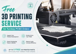
administrator2026-06-03 10:28:422026-06-03 10:31:44Free 3D Printing Service for Turnkey PCBA Orders

https://www.scspcba.com/wp-content/uploads/2026/05/9a2c6d52088asfasg640.webp
640
640
administrator
https://scspcba.com/wp-content/uploads/2026/05/scspcba-home-logo.svg
administrator2026-04-27 10:17:192026-05-18 09:46:42Your PCBA Projects Keep Moving Forward During the Labor Day Holiday

https://www.scspcba.com/wp-content/uploads/2026/05/ai-hardware-pcba-manufacturing.webp
873
1080
administrator
https://scspcba.com/wp-content/uploads/2026/05/scspcba-home-logo.svg
administrator2026-04-24 10:17:082026-05-18 08:14:59AI Hardware PCBA: The Problems You Only Discover After Production Starts
https://www.scspcba.com/wp-content/uploads/2026/05/Box-Build-Printed-Circuit-Board-Assembly-Services.webp
873
1080
administrator
https://scspcba.com/wp-content/uploads/2026/05/scspcba-home-logo.svg
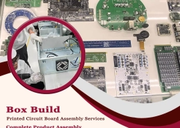
administrator2026-02-25 01:00:182026-05-19 11:00:55Box Build Printed Circuit Board Assembly Services | Complete Product Assembly
In SMT (surface mount technology) production, SMT templates (also known as steel mesh) and various auxiliary fixtures are key tools to ensure welding quality and production efficiency. The surface mount template is used to control the amount and position of solder paste printing, while the fixture is used to fix the circuit board to prevent deformation and ensure the consistency of components during reflow soldering and testing. They may seem simple, but they greatly impact yield and production capacity.
An SMT template, a steel mesh, is a thin precision metal plate with holes corresponding to component pads punched out by laser or chemical etching. The solder paste is evenly applied to the circuit board pads through these holes. The material of the steel mesh is usually stainless steel, which ensures both strength and good corrosion resistance. The thickness of the SMT template and the precision of the holes directly determine the uniformity of solder paste printing, thus affecting the reliability of welding.

In the surface mount technology process, the thickness of the stencil is crucial to the quality of solder paste printing and subsequent soldering effect. The commonly used stencil thickness ranges from 0.1mm to 0.2mm, which is usually determined based on the pad size, device package type and PCB assembly process.
In terms of materials, most SMT stencils are made of 304 or 316 stainless steel, which has excellent corrosion resistance, strength and durability.
A high-quality steel mesh not only improves welding quality but also effectively reduces defect rates, reduces rework and scrap costs, and has a positive impact on the entire SMT manufacturing processing flow.
In the process of SMT patch and printed circuit manufacturing, a high-quality stencil must not only have good dimensional accuracy, but also meet a series of process standards:
Check whether it is compatible with the automatic printing machine. The stencil frame structure must have sufficient rigidity and elasticity to ensure that the stencil is not easily deformed during high-speed printing.
The higher the tension, the better the mesh tension, and the more uniform the solder paste printing. Due to mesh relaxation, there will be no printing offset or uneven solder amount.
Whether there are defects such as deformation, cracks, corrosion or contamination. For high-precision circuit boards, such as circuit board with BGA, each opening must be microscopically inspected to check whether the hole edges are clean and smooth and whether there are burrs or oxidation residues on the inner wall.
Place the PCB to be mounted under the stencil and observe whether the leak hole and the pad are 100% overlapped. If there is misalignment, repeated holes or missing pad positions, it will directly affect the patch accuracy and welding quality.

In the entire process of pcb board assembly, in addition to the role of SMT steel mesh in precise solder paste printing, various auxiliary fixtures also play an irreplaceable role. These fixtures provide precision assurance, thermal deformation control and automatic adaptation support for SMT patch, DIP plug-in, reflow soldering and testing & inspection.
Commonly used on patch machines to ensure stable positioning of circuit boards during the mounting process to prevent component offset or poor soldering due to slight movement. Especially in high-speed SMT mounting, accurate positioning is particularly important for PCB boards with small size or soft board material.
Mostly used in double-sided patch or reflow soldering. Under high-temperature reflow curve, some large-size boards or thin boards are prone to board warping, affecting the quality of solder joints. The fixture support structure can effectively alleviate thermal stress concentration, maintain PCB flatness, and improve soldering reliability. It is particularly suitable for high-density multilayer PCB and rigid-flex PCB.
During the PCBA testing phase, the functional test fixture can quickly achieve the connection between the circuit board and the automated testing equipment, and is compatible with a variety of test probes or connector interfaces. It is a key tool to ensure the consistency and functional integrity of the product before it leaves the factory.
For the double-sided mounting process, a flip-board fixture is also used. This fixture has a flexible structural design and can be used to accurately flip the PCB board after one side is mounted, so that the second side can continue to be mounted and soldered. It is an important auxiliary device to improve production efficiency and accuracy.
In printed circuit board production, SMT templates (stencils) and various fixtures constitute the basic guarantee tools for surface assembly processes. It is not only related to the accuracy of solder paste printing, but also directly affects the consistency of component placement, welding quality and overall production line efficiency, and is the key to achieving high-yield PCB and assembly.
The SMT stencil template is used to accurately print solder paste to the pad area, and finely control the corresponding component package size, pitch and PCB pad shape to ensure the accuracy of subsequent patching. For BGA with high-density wiring, the thickness, opening size and smoothness of the stencil are particularly critical. High-quality laser-cut stencils combined with electropolishing process can significantly improve the efficiency of solder paste release and avoid welding defects such as short circuits and bridges.
Auxiliary fixtures are widely used in multiple stages such as SMT patch, reflow soldering, THT plug-in, flip board, assembly and functional testing (FCT). For example, positioning fixtures ensure that the PCB does not shift during mounting and welding; support fixtures prevent PCB board warping or stress concentration at high temperatures, which is especially important for large-size boards or multi-layer HDI PCBs; test fixtures are used in conjunction with ICT or FCT platforms to achieve fast and efficient electrical testing.
In the process of moving towards automated assembly and lean manufacturing, the standardization and customization of templates and fixtures are particularly important. By connecting with MES system data, they can also help achieve process traceability and improve production transparency.
In summary, SMT templates and fixtures are not only the “invisible protagonists” of PCB Assembly, but also an important guarantee for improving process capabilities, reducing defect rates, and accelerating delivery cycles. A set of reasonably matched and structurally optimized fixture systems is an indispensable core capability for one-stop printed circuit board manufacturers to move towards high-end manufacturing.

Although SMT templates and fixtures seem to be “auxiliary materials”, they play an irreplaceable role in PCB board assembly. From template thickness to fixture structural design, every detail is related to circuit board quality and scspcba PCBA manufacturer image. Only by continuously controlling template processing quality, designing fixtures on demand, and cooperating with advanced mounting technology can we support today’s stringent requirements for high density and high reliability in electronic manufacturing.
https://www.scspcba.com/wp-content/uploads/2026/06/dragon-boat-festival-holiday-notice-scspcba-2026.jpg
873
1080
administrator
https://scspcba.com/wp-content/uploads/2026/05/scspcba-home-logo.svg
administrator2026-06-18 08:47:182026-06-18 08:53:58Dragon Boat Festival Holiday Notice 2026
https://www.scspcba.com/wp-content/uploads/2026/06/free-3d-printing-support-for-turnkey-pcba-prototyping-scspcba.webp
873
1080
administrator
https://scspcba.com/wp-content/uploads/2026/05/scspcba-home-logo.svg
administrator2026-06-03 10:28:422026-06-03 10:31:44Free 3D Printing Service for Turnkey PCBA Orders
https://www.scspcba.com/wp-content/uploads/2026/05/9a2c6d52088asfasg640.webp
640
640
administrator
https://scspcba.com/wp-content/uploads/2026/05/scspcba-home-logo.svg
administrator2026-04-27 10:17:192026-05-18 09:46:42Your PCBA Projects Keep Moving Forward During the Labor Day Holiday
https://www.scspcba.com/wp-content/uploads/2026/05/ai-hardware-pcba-manufacturing.webp
873
1080
administrator
https://scspcba.com/wp-content/uploads/2026/05/scspcba-home-logo.svg
administrator2026-04-24 10:17:082026-05-18 08:14:59AI Hardware PCBA: The Problems You Only Discover After Production Starts
https://www.scspcba.com/wp-content/uploads/2026/05/Box-Build-Printed-Circuit-Board-Assembly-Services.webp
873
1080
administrator
https://scspcba.com/wp-content/uploads/2026/05/scspcba-home-logo.svg
administrator2026-02-25 01:00:182026-05-19 11:00:55Box Build Printed Circuit Board Assembly Services | Complete Product Assembly
When Noemi first contacted SCSPCBA, he was in the early stages of his business, with only a preliminarily completed prototype of a health smartwatch and a long list of imaginative features: heart rate monitoring, blood oxygen tracking, sleep analysis, and fall reminders for the elderly… These features all rely on precise electronic design and stable manufacturing support. However, he knew very well that printed circuit boards and subsequent PCBA manufacturing were the most expensive parts of health AI hardware. Once costs get out of control, mass production plans will fall through. But he also understood that if the design is optimized from the source, the selection is reasonable, the mounting is streamlined, the testing process is standardized, and the PCB board production cost is controlled, this device will have the opportunity to enter thousands of households truly. Noemi is not the only hardware entrepreneur with this problem, and SCSPCBA is the “money-saving key” he found.
The first generation prototype drawings brought by Noemi were fully functional but had messy wiring, complex board layers, and serious redundant interface stacking. After the first round of evaluation, the engineering team of SCSPCBA decided to reconstruct the entire circuit architecture, starting from optimizing printed circuit board design. SCSPCBA streamlined the original 6-layer PCB board to 4 layers, while compressing the routing length and removing unenabled communication interfaces (such as redundant UART and spare BLE module interfaces). This step directly saved more than 20% of the pcb board fabrication cost and the subsequent mounting difficulty of health wearable devices.
While reorganizing the stacking structure of the circuit board, the wiring symmetry and ground layer distribution of key chips were optimized, and the signal integrity and electromagnetic compatibility performance were improved. For Noemi, this means not only saving money, but also ensuring the long-term stable operation of health smart watches in the medical and health field.
PCB board assembly cost-saving techniques are often hidden in the BOM list. Noemi’s original BOM contained multiple imported brand chips, with high unit prices and unstable delivery dates. After evaluation, SCSPCBA’s procurement team proposed suggestions for replacing chips to reduce the manufacturing cost of circuit boards. On the premise of ensuring that the function, compatibility and quality are not affected, more than ten models including power management ICs, logic chips, and some sensor modules were replaced.
For example, the original TI power chip cost more than US$2 per chip. After replacing it with a domestic high-cost-effective brand, the cost dropped to US$0.78 per chip, and the supply cycle was more stable. After evaluating the compatibility of the pcb board layout, we also helped Noemi adjust the pad package so that the replacement components can seamlessly match the original design.
In the end, the cost of the entire set of electronics components was reduced by an average of about 30%. This not only gave Noemi’s production budget some breathing room, but also greatly reduced the risk caused by chip price increases or shortages.

After the PCB circuit board design is finalized, the next key link is the optimization of the SMT surface mount process. Noemi’s original design contains multiple specially-shaped components and non-standard packaged devices, which not only increases the difficulty of programming the surface mount device, but also increases the SMT working hours and surface mount electronic components defect rate.

In medical and health hardware, the reliability of PCB manufacturing and assembly is directly related to the user’s life safety, so Noemi is very cautious in the PCBA testing stage. The initial plan was to manually test each board, but SCSPCBA recommended the use of modular functional test fixtures to replace manual labor, a one-time investment, and long-term savings.
SCSPCBA designed a dedicated FCT test fixture for Noemi, and divided the core functional modules such as heart rate, blood oxygen, vibration, battery charging and discharging into independent test channels, and realized automatic testing and recording after inserting the fixture. Compared with the manual test of 5 minutes for 1 circuit board, the automatic test platform only takes 30 seconds to complete the entire process.
At the same time, for the electrical test part of the printed circuit board, we introduced the ICT (in-circuit test) process to 100% check for problems such as solder joint short circuit, power supply abnormality, and voltage offset. The printed circuit board testing pass rate has increased from the original 94.2% to 99.8%.
Noemi exclaimed: “The average testing cost per board for circuit has dropped from ¥5 to ¥1.6. This is the first time I have seen that pcb board testing can help me save money and improve quality.”
An often overlooked source of cost is the PCBA packaging cost saving solution. Noemi initially adopted a highly customized paper box + EVA foam solution, which was not only costly but also caused waste of transportation volume. SCSPCBA, from the perspective of both brand and cost, recommended that it adopt an anti-static bubble bag + kraft paper outer packaging + printable envelope design solution.
The new packaging takes into account both the electrostatic protection of the circuit board and the product display, with a 40% reduction in volume and a 50% reduction in the cost of a single piece of packaging. More importantly, the packaging uses recyclable materials, which meets the basic requirements of environmental protection in the medical and health field. At the same time, we also assisted him in printing the “Powered by SCSPCBA” cooperation logo on the packaging, saving stickers and manual labeling processes, and further increasing brand endorsement.
This minimalist packaging idea from the factory to the user not only makes Noemi’s products look professional, clean, and thoughtful at the exhibition, but also saves a lot of transportation costs for channel logistics.

Noemi’s project took less than 6 months from start-up to mass production, and the cost of the entire printed circuit board assembly manufacturing was reduced by about 35%, while product stability was doubled.
SCSPCBA is not only a circuit board manufacturer, but also a cost optimization consultant for every link of your product from concept to delivery.
“It’s not about who saves the most, but who saves smarter.” – SCSPCBA Engineering Department
♦ Are you also worried about PCBA costs? Let us provide evaluation and design optimization suggestions for your AI hardware project!
☒ Click to contact an engineer to get a customized printed circuit board solution.
https://www.scspcba.com/wp-content/uploads/2026/06/dragon-boat-festival-holiday-notice-scspcba-2026.jpg
873
1080
administrator
https://scspcba.com/wp-content/uploads/2026/05/scspcba-home-logo.svg
administrator2026-06-18 08:47:182026-06-18 08:53:58Dragon Boat Festival Holiday Notice 2026
https://www.scspcba.com/wp-content/uploads/2026/06/free-3d-printing-support-for-turnkey-pcba-prototyping-scspcba.webp
873
1080
administrator
https://scspcba.com/wp-content/uploads/2026/05/scspcba-home-logo.svg
administrator2026-06-03 10:28:422026-06-03 10:31:44Free 3D Printing Service for Turnkey PCBA Orders
https://www.scspcba.com/wp-content/uploads/2026/05/9a2c6d52088asfasg640.webp
640
640
administrator
https://scspcba.com/wp-content/uploads/2026/05/scspcba-home-logo.svg
administrator2026-04-27 10:17:192026-05-18 09:46:42Your PCBA Projects Keep Moving Forward During the Labor Day Holiday
https://www.scspcba.com/wp-content/uploads/2026/05/ai-hardware-pcba-manufacturing.webp
873
1080
administrator
https://scspcba.com/wp-content/uploads/2026/05/scspcba-home-logo.svg
administrator2026-04-24 10:17:082026-05-18 08:14:59AI Hardware PCBA: The Problems You Only Discover After Production Starts
https://www.scspcba.com/wp-content/uploads/2026/05/Box-Build-Printed-Circuit-Board-Assembly-Services.webp
873
1080
administrator
https://scspcba.com/wp-content/uploads/2026/05/scspcba-home-logo.svg
administrator2026-02-25 01:00:182026-05-19 11:00:55Box Build Printed Circuit Board Assembly Services | Complete Product Assembly
We are very pleased to announce that SCSPCBA will participate in the “MOBiSAD IMEx” exhibition held at Istanbul Expo Center (IFM), Turkey from October 8 to 11, 2025 – an important event for the mobile communications, consumer electronics and emerging technology industries.
☞ Exhibition name: MOBiSAD IMEx 2025
☞ Booth number: 8A-157
☞ Exhibition time: October 8 (Wednesday) to October 11 (Saturday), 2025
☞ Opening hours: 10:00 – 18:00 daily
☞ Exhibition address: Istanbul Expo Center (IFM), Turkey
☞ One-stop service: PCB | SMT/DIP | PCBA | BOM procurement | OEM/ODM | Testing and inspection | BOM and supply chain
☞ Expectation: Welcome to discuss cooperation!

MOBISAD IMEX (Mobile Communication, Consumer Electronics & New Technologies Exhibition) is an annual event hosted by the Turkish Mobile Communication Technology Association, focusing on 5G communications, IoT, consumer electronics, emerging technologies and smart manufacturing. As one of the most influential technology exhibitions in Turkey and even the Middle East, the exhibition attracts technology companies, equipment manufacturers and innovative solution providers worldwide.
As a one-stop PCBA intelligent manufacturing service provider with many years of experience in the field of electronic manufacturing, SCSPCBA will fully demonstrate the company’s strong capabilities and advanced processes in the entire process of PCB design, PCB board fabrication, surface mount technology (SMT/DIP), component procurement, DFM manufacturability testing, printed circuit assembly and testing & inspection, BGA assembly to box build assembly at this MOBISAD IMEX 2025 exhibition. We are committed to providing customers with “end-to-end” intelligent solutions from product conception to mass production to meet the stringent requirements of high-quality, high-efficiency and high-flexibility production.
Experience our AI-driven online fast quotation platform on site. The system combines big data and algorithmic logic to generate accurate quotations, completely eliminating the cumbersome process of traditional manual calculations, and greatly improving procurement efficiency and communication speed. It is especially suitable for small and medium-volume orders, prototype proofing and cross-border collaboration scenarios, truly realizing “fast inquiry, instant quotation”, helping customers seize market opportunities.

We will showcase PCB solutions covering a variety of complex applications, including but not limited to:
All products comply with IPC-610E, RoHS and UL international certification standards and can be widely used in high-end electronics, industrial equipment and high-reliability scenarios.
SCSPCBA has rich experience in patch and assembly, providing flexible manufacturing support from rapid prototyping to medium and large batch production. Specific service highlights include:

SCSPCBA currently has four factories in Vietnam, Shenzhen, Jiangsu, and Jiangxi to achieve production coordination between Southeast Asia and mainland China, and support efficient response and distributed delivery of global orders. At the same time, we have established branches in Wuhan and the United States to further enhance cross-time zone response capabilities and localized service levels.
SCSPCBA’s printed circuit board assembly manufacturing solutions have been successfully applied to multiple industries, including:
Through continuous optimization of circuit board manufacturing processes and strengthening of quality control systems, SCSPCBA has become the preferred partner of many global brands in the field of high-end electronic manufacturing.

Whether you are a local buyer, brand customer, partner or industry researcher, we sincerely invite you to visit SCSPCBA booth 8A-157 to communicate with us face to face and explore how to use intelligent manufacturing technology, flexible supply chain and fast delivery mode to help your products go to market faster, with better cost and more stable quality.
https://www.scspcba.com/wp-content/uploads/2026/06/dragon-boat-festival-holiday-notice-scspcba-2026.jpg
873
1080
administrator
https://scspcba.com/wp-content/uploads/2026/05/scspcba-home-logo.svg
administrator2026-06-18 08:47:182026-06-18 08:53:58Dragon Boat Festival Holiday Notice 2026
https://www.scspcba.com/wp-content/uploads/2026/06/free-3d-printing-support-for-turnkey-pcba-prototyping-scspcba.webp
873
1080
administrator
https://scspcba.com/wp-content/uploads/2026/05/scspcba-home-logo.svg
administrator2026-06-03 10:28:422026-06-03 10:31:44Free 3D Printing Service for Turnkey PCBA Orders
https://www.scspcba.com/wp-content/uploads/2026/05/9a2c6d52088asfasg640.webp
640
640
administrator
https://scspcba.com/wp-content/uploads/2026/05/scspcba-home-logo.svg
administrator2026-04-27 10:17:192026-05-18 09:46:42Your PCBA Projects Keep Moving Forward During the Labor Day Holiday
https://www.scspcba.com/wp-content/uploads/2026/05/ai-hardware-pcba-manufacturing.webp
873
1080
administrator
https://scspcba.com/wp-content/uploads/2026/05/scspcba-home-logo.svg
administrator2026-04-24 10:17:082026-05-18 08:14:59AI Hardware PCBA: The Problems You Only Discover After Production Starts
https://www.scspcba.com/wp-content/uploads/2026/05/Box-Build-Printed-Circuit-Board-Assembly-Services.webp
873
1080
administrator
https://scspcba.com/wp-content/uploads/2026/05/scspcba-home-logo.svg
administrator2026-02-25 01:00:182026-05-19 11:00:55Box Build Printed Circuit Board Assembly Services | Complete Product Assembly
In modern electronic manufacturing, the reliability and consistency of printed circuit assembly directly determine the performance and market reputation of the whole machine. With the continuous upgrading of international quality standards, more and more PCBA manufacturers have adopted authoritative ISO certification systems to standardize production management, raw material procurement and process control to ensure that PCB board production meets the strict requirements of global customers.
Circuit board assembly is a system engineering that covers multiple links, such as component welding, testing, functional verification, and post-aging. Whether it is fully automated placement or inspection requiring manual cooperation, it is like a precision machine that operates efficiently and must be closely coordinated in all links. However, what is often overlooked but equally critical is PCB manufacturers’ quality management system certification, which provides a stable framework and traceability guarantee for the entire production process and is an important basis for customer trust.
Obtaining quality management certifications such as ISO 9001 or ISO 13485 means that the factory meets the internationally accepted quality management system and has traceability, verifiability, and sustainable improvement management capabilities. For printed circuit board manufacturers, such certifications give customers more peace of mind in high-reliability industries such as medical, automotive, and aerospace because they ensure that every node in the entire production process meets strict specifications.

Under the requirements of the ISO system, the printed circuit board production process needs to use a variety of inspection technologies to prevent defects. The main technologies include:
High-resolution cameras capture defects such as solder joints, component offsets, missing parts, etc., automatically compare design drawings, and avoid manual misjudgment.
Monitor the thickness and distribution of solder paste on the pad to prevent printing offset from causing cold solder joints or short circuits.
Perform non-destructive perspective inspection of hidden solder joints such as BGA and QFN to identify voids or poor soldering.
Detect circuit open circuits, short circuits, resistance/capacitance errors, etc. before PCBA is powered on, and quickly find fault points.
Simulate the actual working state, verify the function of the entire board, and ensure mass production consistency.
These functional inspection methods work together to form a complete quality firewall to minimize the outflow of defective products.
ISO certification also requires that the production workshop meet high standards in equipment and management.
For example:
These facilities ensure that PCB patch, plug-in, welding and testing processes can maintain stable and consistent quality, and can trace the abnormalities in each link.
Under the ISO system, operators of electronics manufacturers must pass job certification, including:
And require regular retraining and assessment to ensure that the skill level continues to meet the requirements. ISO emphasizes the sustainable improvement of “people”, so continuously cultivating employee capabilities is part of the certification.
Another highlight of the ISO certification system is traceability. Each batch of PCBA products, from raw materials, production batches to quality inspection reports, will be recorded in the MES or ERP system for later traceability and data analysis. If a return or recall occurs, the affected batch can also be quickly locked, greatly reducing customer risks.

ISO certification has laid a good foundation for circuit board manufacturers to expand their OEM/ODM business. For many international brands, choosing an ISO-certified foundry meets compliance requirements and also reduces cooperation risks.
As a PCBA manufacturer with both ISO9001 and ISO13485 certifications, SCCPCBA printed circuit board manufacturers have one-stop delivery capabilities from design, proofing, small batch trial production, and mass production and can quickly provide customers with high-end customized solutions in medical, automotive, and industrial control.
In today’s fiercely competitive global electronics industry, ISO-certified PCBAs have become an important symbol of measuring a company’s manufacturing capabilities. We can only provide customers with high-reliability and high-consistency circuit board assembly services by combining systematic testing technology, advanced equipment, highly qualified operators, and rigorous production processes. Through continuous improvement and investment, the ISO system helps PCBA manufacturers build a solid bridge between quality and trust.
https://www.scspcba.com/wp-content/uploads/2026/06/dragon-boat-festival-holiday-notice-scspcba-2026.jpg
873
1080
administrator
https://scspcba.com/wp-content/uploads/2026/05/scspcba-home-logo.svg
administrator2026-06-18 08:47:182026-06-18 08:53:58Dragon Boat Festival Holiday Notice 2026
https://www.scspcba.com/wp-content/uploads/2026/06/free-3d-printing-support-for-turnkey-pcba-prototyping-scspcba.webp
873
1080
administrator
https://scspcba.com/wp-content/uploads/2026/05/scspcba-home-logo.svg
administrator2026-06-03 10:28:422026-06-03 10:31:44Free 3D Printing Service for Turnkey PCBA Orders
https://www.scspcba.com/wp-content/uploads/2026/05/9a2c6d52088asfasg640.webp
640
640
administrator
https://scspcba.com/wp-content/uploads/2026/05/scspcba-home-logo.svg
administrator2026-04-27 10:17:192026-05-18 09:46:42Your PCBA Projects Keep Moving Forward During the Labor Day Holiday
https://www.scspcba.com/wp-content/uploads/2026/05/ai-hardware-pcba-manufacturing.webp
873
1080
administrator
https://scspcba.com/wp-content/uploads/2026/05/scspcba-home-logo.svg
administrator2026-04-24 10:17:082026-05-18 08:14:59AI Hardware PCBA: The Problems You Only Discover After Production Starts
https://www.scspcba.com/wp-content/uploads/2026/05/Box-Build-Printed-Circuit-Board-Assembly-Services.webp
873
1080
administrator
https://scspcba.com/wp-content/uploads/2026/05/scspcba-home-logo.svg
administrator2026-02-25 01:00:182026-05-19 11:00:55Box Build Printed Circuit Board Assembly Services | Complete Product Assembly
Design for Manufacturability (DFM) is the practice of designing …
Design for Manufacturability (DFM) is the practice of designing …


