Dragon Boat Festival Holiday Notice 2026
Design for Manufacturability (DFM) is the practice of designing …
Design for Manufacturability (DFM) is the practice of designing …
Design for Manufacturability (DFM) is the practice of designing …
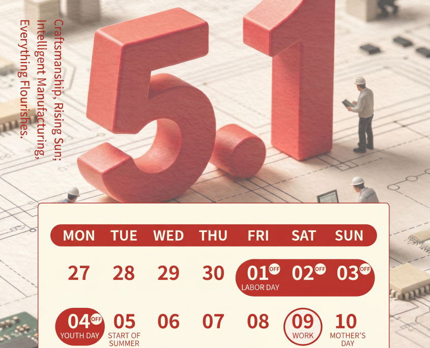
From May 1st to May 4th, our customer service team will be temporarily offline. However, our PCBA online quotation system will remain available 24/7 to ensure your projects continue without interruption.
📌 Visit our website
📌 Upload your BOM or Gerber files to receive an accurate quotation automatically
📌 No waiting required — quotes are generated instantly and available for download
🚀 Orders submitted during the holiday will be prioritized for production scheduling once we resume, helping you accelerate delivery timelines
👉 Get your quotation in advance and start production immediately after the holiday, avoiding unnecessary delays
Thank you for your trust and support.
Wishing you a relaxing and enjoyable holiday!
https://www.scspcba.com/wp-content/uploads/2026/06/dragon-boat-festival-holiday-notice-scspcba-2026.jpg
873
1080
administrator
https://scspcba.com/wp-content/uploads/2026/05/scspcba-home-logo.svg
administrator2026-06-18 08:47:182026-06-18 08:53:58Dragon Boat Festival Holiday Notice 2026
https://www.scspcba.com/wp-content/uploads/2026/06/free-3d-printing-support-for-turnkey-pcba-prototyping-scspcba.webp
873
1080
administrator
https://scspcba.com/wp-content/uploads/2026/05/scspcba-home-logo.svg
administrator2026-06-03 10:28:422026-06-03 10:31:44Free 3D Printing Service for Turnkey PCBA Orders

https://www.scspcba.com/wp-content/uploads/2026/05/9a2c6d52088asfasg640.webp
640
640
administrator
https://scspcba.com/wp-content/uploads/2026/05/scspcba-home-logo.svg
administrator2026-04-27 10:17:192026-05-18 09:46:42Your PCBA Projects Keep Moving Forward During the Labor Day Holiday
https://www.scspcba.com/wp-content/uploads/2026/05/ai-hardware-pcba-manufacturing.webp
873
1080
administrator
https://scspcba.com/wp-content/uploads/2026/05/scspcba-home-logo.svg
administrator2026-04-24 10:17:082026-05-18 08:14:59AI Hardware PCBA: The Problems You Only Discover After Production Starts
https://www.scspcba.com/wp-content/uploads/2026/05/Box-Build-Printed-Circuit-Board-Assembly-Services.webp
873
1080
administrator
https://scspcba.com/wp-content/uploads/2026/05/scspcba-home-logo.svg
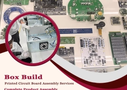
administrator2026-02-25 01:00:182026-05-19 11:00:55Box Build Printed Circuit Board Assembly Services | Complete Product Assembly
Design for Manufacturability (DFM) is the practice of designing …
With the accelerated iteration of electronic products, many OEMs now prefer to choose PCBA suppliers that can provide one-stop “design-manufacturing-assembly” services in order to cope with shortened R&D cycles and market competition pressures.
In the traditional model, companies need to handle multiple stages such as PCB design, board manufacturing, surface mount technology (SMT), and testing separately, resulting in high communication costs and long cycles. However, OEM (Original Equipment Manufacturer) service providers can integrate resources across the entire circuit board manufacturing process to achieve:
This model is particularly suitable for small-to-medium batch and highly complex PCB board production projects
According to reports, PCBA manufacturers with full-process service capabilities will occupy more than 60% of the prototyping and small-batch market.
Modern electronic products place increasingly higher demands on PCB performance, such as high-frequency and high-speed signal processing, high-density wiring, and thermal management. This leads to:
If companies build their own production lines, they need to invest a lot of capital and talent; while choosing a professional OEM can directly utilize their technological accumulation and equipment advantages, reducing trial and error costs.
Considering the following factors, assembling the turnkey box build PCB assembly services is actually more economical:
Industry data show that integrating box build electronics manufacturers can reduce production coordination time by 20% to 35% and shorten the overall product launch cycle.

Box-build assembly refers to the process of integrating the assembled circuit boards into a complete product casing after PCB assembly, and then integrating them with other mechanical components, cables, power supplies, displays, and other components to form a complete electronic device that can operate independently. It is not only the final stage of manufacturing, but also a key link in realizing product functionality and deliverability.
SCSPCBA’s goal is to deliver fully functional products, not just a circuit board
| Aspect | PCB Assembly | Box Build Assembly |
|---|---|---|
| Output | Assembled PCB | Finished product |
| Mechanical integration | ❌ | ✅ |
| Cable & harness | ❌ | ✅ |
| Functional system test | Limited | Full system test |
| Packaging | No | Yes |
| Supply chain complexity | High | Reduced |
| Responsibility ownership | Split | Unified |
PCB assembly focuses on electronics manufacturing, while box build assembly ensures system-level reliability
This is the cornerstone of PCBA cost, directly dependent on the components and PCB materials listed in the BOM.
This includes SMT (Surface Mount Technology), DIP (Digital Integrated Circuit) insertion, and soldering processes. Costs are strongly correlated with the complexity of the printed circuit board manufacturing process.
Small-batch PCB production orders have significantly higher unit costs than mass production due to the high proportion of engineering costs allocated to them.
Different inspection methods correspond to different cost tiers.

PCB box assembly is a crucial step in transforming a product from a “functional circuit board” to a “deliverable complete system,” involving multiple verifications of structure, electrical systems, functionality, and reliability.
The sensitivity of the environment to one-stop box build PCBA manufacturing far exceeds that of PCB manufacturing. Temperature and humidity, cleanliness, and electrostatic discharge protection constitute the three lifelines:
| Control Dimensions | Standard Parameters | Implementation Requirements |
|---|---|---|
| Temperature | 22 ± 2℃ | Precision assembly area temperature control, fluctuation ≤ ±1℃/h |
| Humidity | 45 ± 5% RH | To prevent static electricity buildup and avoid component failure due to moisture absorption |
| Cleanliness | ISO Class 8 | ≥0.5μm particles ≤3,520,000/m³; three-stage filtration system |
| Illumination | Precision range 750–1000 lux | Ensure no part of the visual inspection is missed to avoid misassembly |
| Antistatic Discharge (ESD) | Three-Level Protection System | 1. Antistatic work surface (resistance 10⁶–10⁹Ω)
2. Personnel wearing wrist straps (grounding resistance 1MΩ) 3. Hand disinfection and wearing antistatic clothing every 2 hours. |
| Ground and Equipment | “Three-Free” Standard | Dust-free, oil-free, and water-free; equipment surface particle residue ≤100μg/100cm² |
Prohibited behaviors: Entering the assembly area without wearing anti-static clothing, using ordinary plastic trays, and unpacking sensitive components in non-clean areas.
| Test Category | Test Content | Pass Criteria | Tools/Equipment |
|---|---|---|---|
| Power-on self-test | Instantaneous current and voltage surge upon power-on | No short circuit, no smoke, no abnormal noise | Power load test |
| Basic Function Verification | Button Response, LED Indicators, Display On, Bluetooth/WiFi Connectivity | 100% Function Activation | Automated Test Fixture (FCT) |
| Power Supply Performance | Output Voltages (3.3V/5V/12V) | Fluctuation ≤ ±5% (Full Load) | Digital Multimeter + Load Simulator |
| Temperature Rise Test | Continuous full-load operation for 30 minutes | Key chip temperature rise ≤40℃, casing temperature ≤60℃ | Infrared thermal imager |
| EMC Pre-Compliance |
Radiated Emissions (RE), Conducted Interference (CE) | Passed CISPR 32 Class B initial screening | EMC Receiver |
| Safety Interlocks |
Emergency stop button, light curtain, and access control trigger | Response time ≤ 50ms, system immediately power off | Safety PLC tester |
| Communication Interfaces | USB, Ethernet, RS485; Bit Error Rate | Bit Error Rate < 10⁻⁹ | Signal Analyzer |

One major difficulty in box build projects is quoting complexity.
Costs involve electronics, mechanical parts, labor, and testing simultaneously.
SCSPCBA’s intelligent online quotation platform addresses this by:
The system evaluates:
The box-built PCBA services quote platform dynamically adjusts:
Get a BOM Quote for Your Box Build Project
When products are involved in the following areas, turnkey box build assembly are particularly important:
IoT terminals are generally small in size, multifunctional, and rely on wireless communication, requiring the integration of sensors, MCUs, antennas, and power management modules within a very small space. Box build assembly manufacturer can offer:
Industrial environments present challenges such as vibration, high temperatures, and electromagnetic interference. The assembly of the complete unit must ensure:
A reliable box build assembly manufacturer typically equip themselves with aging chambers and vibration test benches to simulate harsh operating conditions before delivery and expose potential hazards in advance.
From headphones to smartwatches, consumer electronics emphasize both aesthetics and seamless functionality. The value of custom electronic box build assembly services lies in:
Medical devices place extremely high demands on the reliability of their PCBAs, as any failure can be life-threatening. The entire assembly must meet the following requirements:
Automotive electronics face temperature variations ranging from -40°C to 125°C, continuous vibration, and high humidity environments. Special attention is required during assembly:
For example, ADAS radar modules need to remain stable under high-frequency signal transmission; assemblers must have millimeter-wave testing capabilities.

The most effective manufacturing strategy today is not managing multiple vendors but working with a partner capable of supporting:
A unified manufacturing model preserves engineering knowledge and ensures process continuity throughout the product lifecycle.
Get a BOM Quote
Talk to an Engineer About Your Box Build Assembly Project
https://www.scspcba.com/wp-content/uploads/2026/06/dragon-boat-festival-holiday-notice-scspcba-2026.jpg
873
1080
administrator
https://scspcba.com/wp-content/uploads/2026/05/scspcba-home-logo.svg
administrator2026-06-18 08:47:182026-06-18 08:53:58Dragon Boat Festival Holiday Notice 2026
https://www.scspcba.com/wp-content/uploads/2026/06/free-3d-printing-support-for-turnkey-pcba-prototyping-scspcba.webp
873
1080
administrator
https://scspcba.com/wp-content/uploads/2026/05/scspcba-home-logo.svg
administrator2026-06-03 10:28:422026-06-03 10:31:44Free 3D Printing Service for Turnkey PCBA Orders
https://www.scspcba.com/wp-content/uploads/2026/05/9a2c6d52088asfasg640.webp
640
640
administrator
https://scspcba.com/wp-content/uploads/2026/05/scspcba-home-logo.svg
administrator2026-04-27 10:17:192026-05-18 09:46:42Your PCBA Projects Keep Moving Forward During the Labor Day Holiday
https://www.scspcba.com/wp-content/uploads/2026/05/ai-hardware-pcba-manufacturing.webp
873
1080
administrator
https://scspcba.com/wp-content/uploads/2026/05/scspcba-home-logo.svg
administrator2026-04-24 10:17:082026-05-18 08:14:59AI Hardware PCBA: The Problems You Only Discover After Production Starts
https://www.scspcba.com/wp-content/uploads/2026/05/Box-Build-Printed-Circuit-Board-Assembly-Services.webp
873
1080
administrator
https://scspcba.com/wp-content/uploads/2026/05/scspcba-home-logo.svg
administrator2026-02-25 01:00:182026-05-19 11:00:55Box Build Printed Circuit Board Assembly Services | Complete Product Assembly
Design for Manufacturability (DFM) is the practice of designing …
In PCB assembly, most failures are not design errors but process-related defects. According to IPC field data, over 60% of electronic failures originate from soldering defects, component placement errors, or insufficient process control.
During the PCB manufacturing assembly, small welding errors or misplaced components may lead to functional failure of the entire circuit board. Through first article inspection (FAI), process accuracy can be verified before mass production, preventing a large number of defective circuit board due to design or operational errors, and significantly reducing material and labor waste. Research shows that first-piece inspection can control the defective rate below 1%, greatly improving production economy.
Electrical performance testing includes continuity testing, insulation resistance testing, and signal defect analysis at high frequencies, which can identify potential problems such as open circuits, short circuits, and crosstalk. These tests not only verify that the circuit works as designed but also identify performance defects caused by improper wiring, ensuring that the PCB assembly is stable and reliable in actual applications.
For fields with high reliability requirements such as medical care, automobiles, and industrial control, PCBs must withstand environmental reliability conditions such as temperature and humidity cycles, vibration, shock, and salt spray. This type of test simulates long-term use, evaluates the circuit board’s ability to withstand extreme environments, and ensures the service life and safety of the printed circuit board production. It is a key step in passing industry certifications (such as ISO 9001, IPC standards).
Automated means such as automatic optical inspection (AOI), in-circuit testing (ICT) and functional testing (FCT) can achieve efficient and consistent quality control on SMT and DIP production lines. These tests not only detect accuracy, but also generate data records that can be supplemented and improved, while continuously optimizing the process and improving the overall manufacturing level.
Complying with international standards such as IPC-A-610, ISO 9001, UL, ROSH etc. can not only standardize and implement quality and technology, but also help companies establish a complete quality management system. PCB boards that meet standards are more likely to earn customers’ trust and compete more effectively in the global market.

Reliable PCBA testing services must rely on authoritative industry standards and strict quality benchmarks to ensure the safety, reliability and compliance of PCB board throughout the entire life cycle of design, manufacturing, assembly and application.
IPC-A-610 is the most widely used assembly quality acceptance standard in the global electronics manufacturing field. It defines three-level product classification and acceptance criteria from consumer to high-reliability products.
Key inspection items include: solder joint shape, pin coplanarity, virtual soldering/bridging identification, intermetallic compound (IMC) thickness control (1–3μm), etc.
IATF 16949 is a quality management system standard unique to the automotive industry
Circuit board manufacturing such as automotive light panels, ECUs, and ADAS systems must meet this standard before they can enter the OEM supply chain.
Complying with UL + RoHS at the same time means that the circuit board is both safe and environmentally friendly, improving the competitiveness in the international market.
| ISO standard | application areas | core requirements |
|---|---|---|
| ISO 9001 | General quality management | Establish a PDCA cycle to ensure that the process is stable and controllable |
| ISO 14001 | Environmental management | Control waste emissions, energy consumption, and use of hazardous substances |
| ISO 13485 | Medical equipment | Emphasize biocompatibility, sterile processing, and traceability |
| ISO 45001 | Occupational health and safety | Ensure the safety of production personnel |

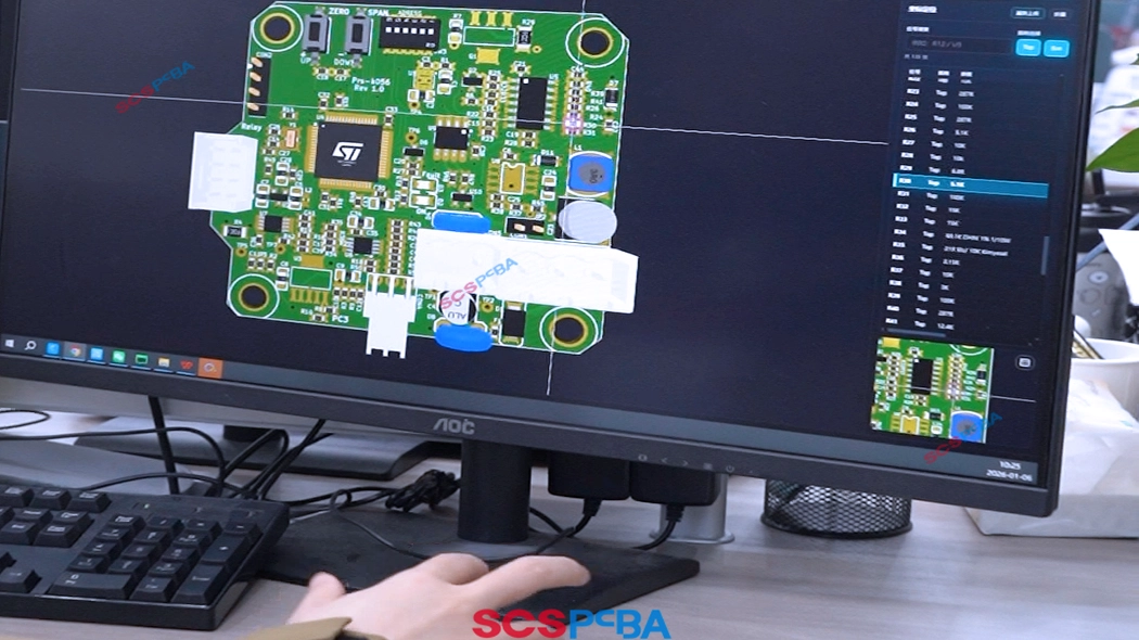
In the SCS PCBA circuit board assembly, the quality control of the SMT and DIP assembly processes is combined with the MES system through detection technologies such as SPI, AOI, and X-Ray to achieve full-process closed-loop control from process foundation to finished product quality.
SPI (Solder Paste Inspection) performs 3D measurements of solder paste thickness, volume, and offset after printing and before patching to detect insufficient solder paste, bridging risks, and template problems to ensure a reliable welding foundation.

AOI (Automatic Optical Inspection) performs inspections after component placement and after reflow soldering, identifying issues such as missing components, misalignment, reversed polarity, solder bridging, and insufficient soldering.

X-ray inspection is used to detect packaging types that cannot be observed with the naked eye or AOI (Automated Optical Inspection), such as bottom solder joints of BGA, CSP, and QFN packages.

The MES system integrates inspection data from SPI, AOI, and X-Ray equipment with the production process, building a complete quality data chain.
SCSPCBA introduces the MES system into the SMT process, combining it with SPI + AOI + X-Ray triple inspection. A process history file is created for each printed circuit board production, enabling precise defect location and rapid containment.
Not all projects need the same testing depth.
| Test Type | Best For | Risk Coverage |
|---|---|---|
| ICT | Medium–high volume boards | Open/short, component value |
| FCT | Function-critical products | Real operating behavior |
| Burn-In | Power & industrial | Early failure screening |
| Environmental | Automotive/outdoor | Thermal & humidity stress |
SCSPCBA has established a dedicated testing laboratory independent of the PCB board production line to ensure that the testing environment is free from production interference and to achieve comprehensive quality control throughout the entire process. The laboratory adopts a partitioned management model, encompassing functional testing, environmental simulation, fault analysis, and clean repair areas. It is equipped with an intelligent monitoring system that records test data in real time and integrates with the production system.


 on the finished circuit boards.")
PCB assembly and testing are not single processes but rather a multi-level quality control system that spans the entire process from raw material warehousing to finished product shipment. The following is SCSPCBA’s core testing process:
Common tools: Optical microscope, automatic optical inspection (AOI) system, hygrometer
| Manufacturing Process | Inspection Items |
|---|---|
| Solder paste printing | Printing thickness, misalignment, leakage, blurring |
| SMT Assembly | Component presence/absence, positional deviation, polarity reversal, and lifting/tilting |
| Reflow soldering | Temperature profile monitoring, wettability, bridging, cold solder joints |
| Wave soldering | Solder joint fullness, solder penetration rate, shadowing effect |
Real-time monitoring can effectively intercept over 90% of early-stage defects.
(5) OQA Inspection and Final Approval
(6) Packaging and Shipment Traceability
These tests ensure the long-term stable operation of the PCB board assembly in complex environments and form the basis for certifications such as ISO 9001 and IATF 16949.

| Application areas | core standards | Test items |
|---|---|---|
| Automotive electronics | IATF 16949 + IPC-A-610 Class 3 | Thermal cycling, vibration, salt spray, PPAP files |
| Medical equipment | ISO 13485 + ISO 10993 + IPC-A-610 | Ionic contamination, chemical resistance, and biocompatibility |
| Industrial control | IPC-A-610 Class 2 + ISO 9001 | Continuity test, insulation resistance, high temperature aging |
| Aerospace | MIL-P-45204 + IPC-A-610 Class 3 | Gold layer thickness ≥0.76μm, no corrosion in salt spray for 96 hours |
| Outdoor communications | IEC 60068-2-30 + ISO 9227 | Temperature and humidity cycle, UV aging, salt spray test |
https://www.scspcba.com/wp-content/uploads/2026/06/dragon-boat-festival-holiday-notice-scspcba-2026.jpg
873
1080
administrator
https://scspcba.com/wp-content/uploads/2026/05/scspcba-home-logo.svg
administrator2026-06-18 08:47:182026-06-18 08:53:58Dragon Boat Festival Holiday Notice 2026
https://www.scspcba.com/wp-content/uploads/2026/06/free-3d-printing-support-for-turnkey-pcba-prototyping-scspcba.webp
873
1080
administrator
https://scspcba.com/wp-content/uploads/2026/05/scspcba-home-logo.svg
administrator2026-06-03 10:28:422026-06-03 10:31:44Free 3D Printing Service for Turnkey PCBA Orders
https://www.scspcba.com/wp-content/uploads/2026/05/9a2c6d52088asfasg640.webp
640
640
administrator
https://scspcba.com/wp-content/uploads/2026/05/scspcba-home-logo.svg
administrator2026-04-27 10:17:192026-05-18 09:46:42Your PCBA Projects Keep Moving Forward During the Labor Day Holiday
https://www.scspcba.com/wp-content/uploads/2026/05/ai-hardware-pcba-manufacturing.webp
873
1080
administrator
https://scspcba.com/wp-content/uploads/2026/05/scspcba-home-logo.svg
administrator2026-04-24 10:17:082026-05-18 08:14:59AI Hardware PCBA: The Problems You Only Discover After Production Starts
https://www.scspcba.com/wp-content/uploads/2026/05/Box-Build-Printed-Circuit-Board-Assembly-Services.webp
873
1080
administrator
https://scspcba.com/wp-content/uploads/2026/05/scspcba-home-logo.svg
administrator2026-02-25 01:00:182026-05-19 11:00:55Box Build Printed Circuit Board Assembly Services | Complete Product Assembly
Design for Manufacturability (DFM) is the practice of designing …
Industrial control printed circuit board assembly carries and implements crucial functions such as signal sensing, data processing, logical decision-making, and instruction execution in industrial automation systems. Specifically, this is reflected in the following aspects:
Industrial control PCBA is the hardware foundation of core control equipment such as PLCs (Programmable Logic Controllers), DCS (Distributed Control Systems), servo drives, and human-machine interfaces (HMI). It provides a physical mounting platform and electrical connection pathways for all electronic components, including microprocessors (MCU/MPU), memory, sensor interfaces, communication chips, and power modules.
The circuits on the PCBA receive weak analog signals from sensors such as temperature, pressure, and position, and preprocess them through amplification, filtering, and isolation (such as using optocouplers) to eliminate electromagnetic interference in the industrial environment.
Industrial control PCBAs must be designed and manufactured using more durable materials and stricter process standards to withstand harsh industrial environments such as high and low temperatures, humidity, dust, vibration, and strong electromagnetic interference.
Industrial control PCBA is widely used in:
PLCs are the brains of industrial automation, and their core is highly reliable PCB assembly and manufacturing. These circuit boards are responsible for receiving signals from sensors, executing preset logic programs, and outputting control commands to actuators such as motors and valves, thereby achieving automated control of production lines and machinery.
Whether monitoring temperature, pressure, flow rate, liquid level, or other physical parameters, industrial sensors and measuring instruments rely on precise PCB fabrication and assembly to collect weak analog signals, amplify them, and perform analog-to-digital conversion, then output or transmit the processed data. These PCB manufacturing assemblies require high precision and resistance to industrial environmental interference.
The joint drives, motion control, and sensing systems of industrial robots all rely on assembly boards. They are used to process data from encoders, torque sensors, etc., run complex motion control algorithms, and drive servo motors to achieve precise and coordinated movements.
In various industrial equipment, from large pumps to precision machine tools, PCBAs are used to build motor drivers and controllers, enabling precise control of motor speed, torque, and position.
PCBA manufacturing is used to manufacture communication devices such as industrial Ethernet switches and fieldbus gateways (e.g., Profibus, Modbus), ensuring stable and real-time transmission of control signals and data in the factory network.
The touch screens, control panels, and operator consoles used by factory operators all contain circuit board assemblies, which are used to process user input, display operating status and alarm information, and communicate with the higher-level control system.
Industrial control boards face strong electromagnetic interference (EMI) and unstable power environments. Key requirements include:
A single unstable solder joint or layout flaw can cause system downtime, making high-reliability industrial printed circuit board assembly manufacturing essential.

SCSPCBA operates 5 SMT production lines, specifically configured to support industrial control PCBA, automotive electronics, and medical electronics—not just consumer products.
This SMT line is where industrial-grade PCBA requirements are truly met, rather than adapted from consumer production.
Primarily used for consumer electronics, these lines are strictly isolated from industrial control projects.
Industrial control PCBA is not mixed with high-speed consumer orders, ensuring:
Designed for:
This allows OEM & ODM customers to move smoothly from prototype → pilot → mass production without changing manufacturing logic.
High capacity ensures:
Stable delivery for long-term industrial PCBA projects
Scalability for automation customers entering mass circuit board manufacturing production
Industrial control boards often include power components, connectors, relays, transformers, which require reliable through-hole assembly.
SCSPCBA provides 2 DIP production lines, optimized for industrial reliability.
Dedicated to small-batch, high-reliability orders, including:
Advantages for industrial PCBA:
This is especially important for PLC boards, control modules, and power control PCB board production.
Mainly used for:
Industrial projects are selectively assigned, avoiding unnecessary printed circuit board manufacturing process risk.
Used for:
Manual soldering is controlled, documented, and inspected—not used as a shortcut, but as a precision supplement for industrial control PCBA.
Ensures reliability without sacrificing delivery time.

SCSPCBA operates 2 dedicated assembly & testing lines, essential for industrial control products that require functional validation, not just visual inspection.
6 functional test stations supports:
Functional testing is critical for industrial PCB assembly, where field failure is unacceptable.
20 assembly workstations supports:
This enables PCBA + box build services for automation and industrial control systems.
SCSPCBA’s manufacturing data demonstrates process maturity, not labor dependency.
This indicates:
For industrial control PCBA, process stability is more important than sheer labor scale
At SCSPCBA, DFM is implemented as a manufacturing-driven design optimization system, ensuring that potential risks are identified and eliminated before mass pcb assembly production begins.
SCSPCBA DFM System for Industrial Control PCBA
SCSPCBA provides a structured DFM analysis workflow, specifically tailored for industrial PCB assembly and automation PCBA, covering the following critical dimensions
Industrial control PCBA often operates in environments with electrical noise, thermal stress, and long duty cycles.
SCSPCBA evaluates:
Improved signal integrity, reduced EMI risk, and enhanced long-term stability for industrial control PCB assembly.
Solder joint reliability is a crucial factor in automation PCB assembly, particularly for applications that are prone to vibration and require high current.
DFM checks include:
Lower risk of cold solder joints, tombstoning, voiding, and long-term fatigue failure.
Thermal issues are one of the most common root causes of industrial electronics failure.
SCSPCBA’s DFM system analyzes:
Compatibility with enclosure-level heat dissipation
Industrial projects often require long lifecycle support and supply chain stability.
SCSPCBA performs:
Reduced supply chain disruption risk and improved cost control for industrial PCB fabrication and assembly projects.
Unlike factories that address issues during production, SCSPCBA applies a DFM-first approach, where:
This approach significantly reduces:
SCSPCBA’s MES system enables:
Component batch-level traceability
Real-time production data monitoring
Process parameter recording for each PCB fabrication process
Quality history tracking for audits and after-sales support
This is especially critical for OEM and ODM industrial PCBA projects
To start an industrial PCB assembly quotation, customers simply upload:
Based on these file and list, the system generates a fast and transparent preliminary quotation covering:
This enables OEM and ODM customers to quickly evaluate project feasibility and budget.
SCSPCBA’s quotation system is built on actual industrial manufacturing data, including:
As a result, customers receive:
This is critical for industrial PCB assembly and automation PCB projects, where late-stage changes create high risk and cost.
The PCBA online quotation system is particularly valuable for:
Combined with SCSPCBA’s DFM and MES systems, the quotation process becomes part of a controlled and traceable manufacturing workflow.
If you are planning an industrial control PCBA or automation PCB assembly project, SCSPCBA’s online quotation system provides a fast, transparent, and engineering-backed starting point.
For OEM and ODM clients, the right partner should offer:
SCSPCBA supports OEM and ODM industrial control PCBA from prototype to mass production, helping customers shorten time-to-market while maintaining quality.
An industrial automation manufacturer (OEM) uses products for factory control systems that operate in high-interference and high-load environments for a long time and have extremely high requirements for stability, maintainability and consistency of equipment.
The customer uploaded the following files through SCSPCBA’s Industrial Control PCBA Online Quotation System:
The system quickly generated a preliminary quotation for Industrial PCB Assembly, covering:
Before confirming manufacturing of the industrial control PCBA board, the SCSPCBA engineering team initiated a DFM (Design for Manufacturability) analysis based on the customer documentation.
DFM focuses on discovering and optimizing the following issues:
PCBA enters the later stage of production, and SCPCBA’s MES monitors the entire process.
The MES system implemented in this industrial control PCBA project:
One-off small batch production
The functional test pass rate is significantly higher than the customer’s previous projects
No on-site abnormalities caused by manufacturing issues
Smoothly enter the subsequent mass production stage
Customer feedback:
“SCPCBA’s online quotation is not a simple price calculation, but takes engineering, manufacturing and risk control into consideration, which is very critical for industrial control PCBA.”
If you are developing or upgrading industrial control PCBA/automated PCB assembly projects:
Upload your PCB file + BOM list + assembly file

Industrial PCB assembly focuses on stability, anti-interference, long lifecycle components, and strict process control, while consumer PCBA prioritizes cost and speed.
Industrial control PCBA is widely used in:
Key requirements include:
Common types include:
SCSPCBA’s DFM system includes:
Yes. SCSPCBA supports prototypes, pilot runs, and scalable mass production, allowing OEM and ODM customers to grow without changing suppliers.
Typical testing includes:
Yes. SCSPCBA offers an industrial PCBA online quote system for fast and transparent pricing based on Gerber files, BOM, and assembly data.
Absolutely. SCSPCBA supports both OEM and ODM industrial PCBA, offering DFM support, supply chain management, testing, and optional box build services.
Yes. All industrial quotations are reviewed by engineers after system pricing, ensuring manufacturability, reliability, and realistic lead times.
https://www.scspcba.com/wp-content/uploads/2026/06/dragon-boat-festival-holiday-notice-scspcba-2026.jpg
873
1080
administrator
https://scspcba.com/wp-content/uploads/2026/05/scspcba-home-logo.svg
administrator2026-06-18 08:47:182026-06-18 08:53:58Dragon Boat Festival Holiday Notice 2026
https://www.scspcba.com/wp-content/uploads/2026/06/free-3d-printing-support-for-turnkey-pcba-prototyping-scspcba.webp
873
1080
administrator
https://scspcba.com/wp-content/uploads/2026/05/scspcba-home-logo.svg
administrator2026-06-03 10:28:422026-06-03 10:31:44Free 3D Printing Service for Turnkey PCBA Orders
https://www.scspcba.com/wp-content/uploads/2026/05/9a2c6d52088asfasg640.webp
640
640
administrator
https://scspcba.com/wp-content/uploads/2026/05/scspcba-home-logo.svg
administrator2026-04-27 10:17:192026-05-18 09:46:42Your PCBA Projects Keep Moving Forward During the Labor Day Holiday
https://www.scspcba.com/wp-content/uploads/2026/05/ai-hardware-pcba-manufacturing.webp
873
1080
administrator
https://scspcba.com/wp-content/uploads/2026/05/scspcba-home-logo.svg
administrator2026-04-24 10:17:082026-05-18 08:14:59AI Hardware PCBA: The Problems You Only Discover After Production Starts
https://www.scspcba.com/wp-content/uploads/2026/05/Box-Build-Printed-Circuit-Board-Assembly-Services.webp
873
1080
administrator
https://scspcba.com/wp-content/uploads/2026/05/scspcba-home-logo.svg
administrator2026-02-25 01:00:182026-05-19 11:00:55Box Build Printed Circuit Board Assembly Services | Complete Product Assembly
Design for Manufacturability (DFM) is the practice of designing …


