How PCB Design Decisions Affect PCBA Manufacturing Yield, Cost, and Reliability
PCB design decisions shape the conditions under which a board can be fabricated, assembled and tested. Pad geometry, component spacing, via structure, stack-up and test access all deserve attention before production. Their effect depends on the actual design and manufacturing route; a single layout change cannot promise a fixed yield improvement or cost reduction.
For an AI hardware project, connect those decisions to the intended product requirements early. The useful discussion is about the board, its components and its verification plan. An AI application label does not define the manufacturing limits or establish the product’s reliability requirements.
Begin with the manufacturing limits and a clear revision
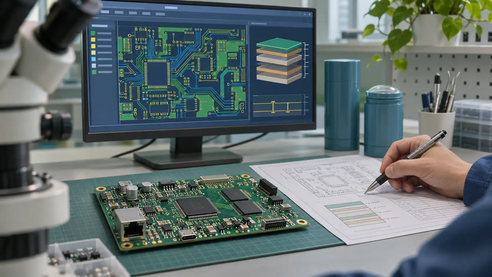
Design for manufacturability brings production-process limitations into the design stage. A layout can be electrically feasible yet difficult to manufacture. Each fabricator has process limits for features such as line width, spacing, via dimensions and impedance tolerance, so configure rules against the capabilities proposed for the build.
The PCBA DFM checklist provides a practical starting point for reviewing fabrication, assembly and test access. This article focuses on the decisions behind those checks: what to change, which tradeoffs to discuss and what to confirm before releasing files.
Review the design files, BOM and assembly drawings together. Ask the fabricator and assembler to identify the file revision used for their feedback. If a layout change follows the review, submit the updated package and obtain confirmation of the affected items. Make the release decision against that package rather than an earlier quotation or drawing.
Review pads and placement access as assembly decisions
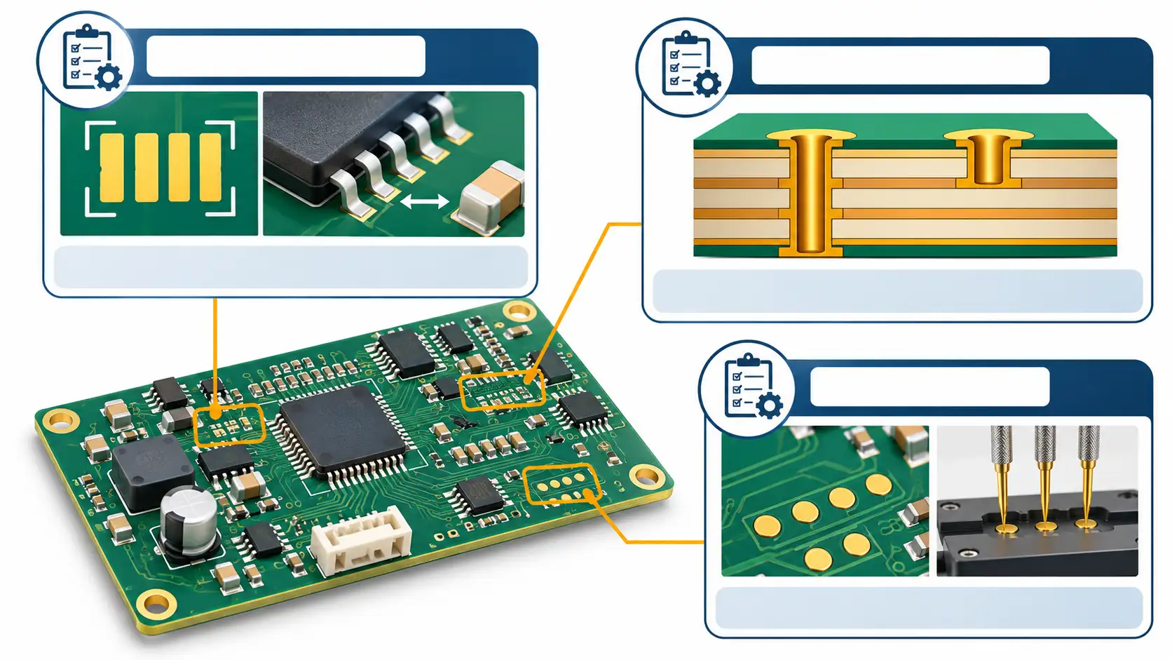
DFM review can examine whether the pad design is reasonable and whether component spacing meets placement-machine requirements. It can also consider test-point layout for ICT or functional-test access. These are design questions with manufacturing consequences, so involve the assembly team while changes remain practical.
Ask for specific feedback. Which footprint needs review? Which component pair creates an access question? Does the proposed correction affect another requirement? Include polarity and orientation markings in the review package so the intended assembly is clear. Avoid replacing these questions with a universal spacing rule that has not been checked for the selected components and process.
A footprint change should be discussed alongside the actual part and assembly drawing. Ask the engineer to confirm the manufacturer’s recommended land pattern and the assembler’s process assumptions. Treat that confirmation as a design decision, with its revision and owner recorded, rather than assuming that a successful CAD check settles assembly suitability.
This also gives purchasing a more precise question when a substitute component is proposed. Ask whether the alternate uses the approved footprint and whether its assembly and test assumptions remain acceptable. Keep the approval tied to the exact part and revision; an available replacement is still a proposal until the responsible team accepts it.
Balance via density and stack-up against process complexity
Blind and buried vias can improve routing capability while increasing manufacturing complexity. Interlayer alignment, microvia aspect ratio, stack-up, impedance control and laser-drilling limitations are among the issues that can affect yield and reliability during mass production. Review the chosen structure with the fabricator after layout.
The stack-up also affects signal integrity, power integrity, electromagnetic compatibility, manufacturing yield and cost. That makes it a shared electrical and manufacturing decision. Ask which layer arrangement and via structure the supplier evaluated, and whether a proposed alternative changes the electrical assumptions.
Bare-board cost varies with layer count, materials, copper thickness, surface finish, hole density, circuit accuracy and order volume. Compare feasible alternatives against the complete requirement set. Reducing one feature is not enough reason to accept a design change if the product’s electrical or verification requirements remain unresolved.
For AI computing boards, bring the real electrical, thermal and mechanical requirements to that discussion. Ask the design team to state operating conditions, allowable limits and the planned verification. Select the final construction against those requirements and the fabricator’s confirmed capabilities, rather than treating a more complex stack-up as an automatic quality upgrade.
Consider the production panel before fixing the board outline
Panelization can improve material utilization and SMT equipment capacity and reduce the processing cost allocated to each board. The amount of benefit depends on the layout and production arrangement. Ask the assembler to review the proposed panel together with its handling, inspection, testing and separation requirements.
Board edges, fiducials and separation features belong in that conversation. Request the proposed arrangement and identify who approves it. If a panel change is offered as a cost saving, ask which assumption changed and whether the same finished-board requirements still apply.
The PCBA cost breakdown guide helps turn that discussion into a comparable quotation. Keep revision, quantity, materials and test scope consistent when comparing options. Otherwise, an apparent design saving may simply reflect a different set of quoted responsibilities.
Design test access before the test fixture is agreed
Design for testability evaluates test coverage and probe accessibility. Test points are pads reserved for contact during ICT or flying-probe testing. Coverage, unobstructed access and compatibility with automated test equipment are design considerations, not details to leave entirely to final inspection.
Discuss which board-level conditions the test plan must check and whether the proposed layout allows the required contact. If access is restricted, ask the test engineer to explain the coverage consequence and the available design or test options. Keep that decision visible in the release review.
Inspection methods also have different boundaries. SPI checks solder-paste printing. AOI cannot directly observe joints concealed beneath BGA or QFN components; X-ray can image hidden joints. ICT checks board interconnections and component parameters, while FCT verifies intended functions under simulated use conditions.
Choose the methods and acceptance criteria around the product requirements. Passing ICT or FCT confirms the corresponding tested items. Aging, fatigue or environmental testing may still be needed, depending on the product mission profile and reliability specifications. Test access supports a verification strategy; it does not by itself prove field life.
Include BOM decisions in the design-to-cost review
Component cost can vary with sourcing, scarcity, package precision, procurement quantity and market-price changes. BOM review can also consider lifecycle, approved alternatives and lead-time risk. A design review that considers only bare-board cost leaves those purchasing questions unanswered.
Ask which component decisions remain flexible and who can approve an alternate. Compare a proposed change against the intended circuit, package and test requirements before accepting its quoted price. Do not assume that the lowest component line price gives the lowest complete build cost.
Problems identified during design verification generally have lower modification costs. If design defects emerge after mass production begins, rework costs may increase. This is a reason to request specific feedback early, not a basis for promising a universal saving from DFM.
Use AI-assisted quotation with an engineering feedback loop
SCSPCBA lists AI Gerber recognition, BOM intelligent matching and automatic price calculation among its online PCB/PCBA quotation functions. AI computing is one of its application areas. These are useful subjects to raise when preparing an inquiry for an AI hardware project.
Submit complete manufacturing files and a structured BOM, then ask the engineering team to confirm the interpreted assumptions. Keep proposed design changes, approved parts and the final build revision distinguishable. AI-assisted recognition does not replace engineering sign-off or establish a predicted yield result.
The turnkey PCBA manufacturing process shows how design information connects with purchasing, fabrication, assembly and testing. Use that sequence to identify when a design decision must be settled before a downstream activity proceeds.
A practical pre-release review
Before release, ask the responsible teams to confirm the following items against the same file package.
Keep unresolved questions specific enough to answer. Name the affected location or component, the proposed action and the person responsible for approval. If the design stays unchanged, record the accepted requirement or condition. The goal is a release decision that engineering, purchasing and production can all reference for this build.
| Decision area | Question to close |
| Design revision | Which files, BOM and drawings define the build? |
| Assembly | Have pad, spacing, orientation and access questions been resolved? |
| Fabrication | Has the fabricator reviewed the stack-up and via structure? |
| Panel | Who approves handling and separation arrangements? |
| Verification | What will inspection and testing cover? |
| Changes | Who approves proposed design or component changes? |
Send the current package and open questions to SCSPCBA for a preliminary manufacturing review. Include target quantity and test requirements so the discussion can address the intended build and quotation scope.
FAQ
Can a layout change guarantee better PCBA yield?
No. Review its effect against the actual design, process and verification requirements. Do not assign a fixed improvement without project data.
Are blind and buried vias always the better choice?
They can improve routing capability but add manufacturing complexity. Confirm whether the design needs them and whether the proposed process is suitable.
Should test points be reviewed before production?
Yes. Test coverage and probe access are DFT considerations. Agree the intended test strategy while the layout can still be reviewed.