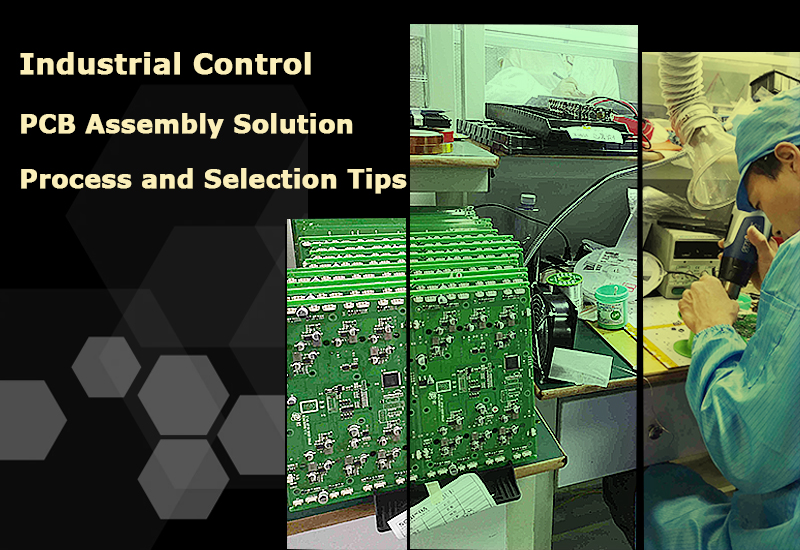
Below, we will introduce the production process of multi-layer PCB fabrication in detail, as well as its application in industrial control.
Use printed circuit design software to design inner lines. When designing, it is necessary to consider factors such as the function, performance requirements, and spatial layout of the PCB. After the design is completed, the graphic file of the inner line needs to be generated.
In industrial control systems, complex printed circuit layouts are usually required, including microcontrollers, sensors, communication interfaces, etc. The designer uses CAD software to create circuit diagrams and layouts to determine the connection method and distribution of the inner line.
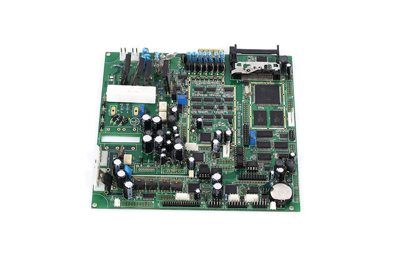
Multi-layer plates usually include inner and outer layers. The inner layers are buried in the middle of the plate, while the outer layer is located on the surface of the plate. Multi-layer boards usually involve pressing these layers together. The typical multi-layer structure includes two outer layers, and the number of inner layers in the middle can be changed according to needs. Each layer contains copper foil for lines.
Transfer the designed inner line graphics to the copper foil board. First of all, apply the light-sensitive material to the copper foil plate, and then transfer the inner line graphics to the copper foil plate through the photoresist.

After the inner plate is made, the next step is plating, and the copper foil will be thickened to form a reliable line. The chemical process is used to use the acrum by the anode and the copper is deposited on the line pattern.
Use the etching liquid to erode the non-light copper foil and leave the inner line graphics. The etching process needs to control the time and temperature to ensure the accuracy and quality of the line graphics.
After the etching is completed, the copper foil board needs to be cleaned to remove the residual etching solution and light-sensitive material. Then, the quality of the inner line needs to be checked, including the width, spacing, and connectivity of the line.
After production of the inner line board is ready, put multiple inner boards together with the outer plate, and then use high temperature and pressure to press the layer pressure. This will ensure that the connection between each layer is firm. Then drill holes at the specified position and gold at the position of the drill to improve the conductivity and corrosion resistance of the PCB to form the connection point of the printed circuit board.
The lines on the outer plate are usually connected to the lines on the inner plate. Make the outer line according to the same step. After completing the layer pressure, the multi-layer board may need to perform the processing of final cutting, bending and positioning of holes.
Multi-layer PCB fabrication needs to be tested to ensure the correctness of the line. Common test methods include connectivity testing and electrical testing. Quality control also includes the size of the line, the position of the hole, etc.

The application of multi-layer PCB assembly has a wide range of applications in the industrial control system, playing a key role in automated equipment, industrial robots, and industrial networks. The continuous progress and innovation of these technologies help improve the performance, reliability and intelligence level of the industrial control system, thereby meeting the development of industrial needs.
· Control logic Implementation
Multi-layer PCB technology can accommodate complex control logic, including the collection of sensor data, data processing and decision-making formulation. This helps to achieve a high-level automation process, improve production efficiency, and reduce artificial intervention.
· Communication Interface
Multi-layer PCB manufacturing can integrate various communication interfaces, such as Ethernet, Modbus, Profibus, etc. to achieve data sharing and remote monitoring between devices. This is very important for the collaboration of automation equipment.
· Accurate Exercise Control
Industrial robots usually need highly accurate exercise control to perform complex tasks, such as assembly, welding and packaging. Multi-layer PCB assembly manufacturing can support high-speed, high-precision motor control and motion planning, thereby improving the work efficiency and accuracy of robots.
· Sensor Integration
Multi-layer PCB can be used to integrate various sensors, such as laser rangers, visual systems, and force sensors to achieve the environmental perception and adaptability of the robot.
· High-speed Data Transmission
In industrial networks, the rapid transmission of data is essential for real-time monitoring and decision-making. The multi-layer electronic board can support high-speed data bus and communication protocols to ensure real-time transmission and processing of data.
· Network Stability and Security
Multi-layer PCB circuit boards can also integrate security functions, including firewalls, encryption, certification, and access control, to improve the stability and security of the industrial network, and protect key data and systems from the infringement of network threats.

Multilayer PCB circuit boards can improve the stability and security of industrial control networks
The production of the multi-layer PCB is a complex process that requires precise equipment and strict quality control. Through this process, we can make multi-layer boards with excellent performance and high reliability to meet the needs of various complex circuits With the development of industrial automation and digitalization, the design and manufacturing technology of multi-layer boards have continued to improve. Provide more innovation and solutions to provide strong support for our production and life.