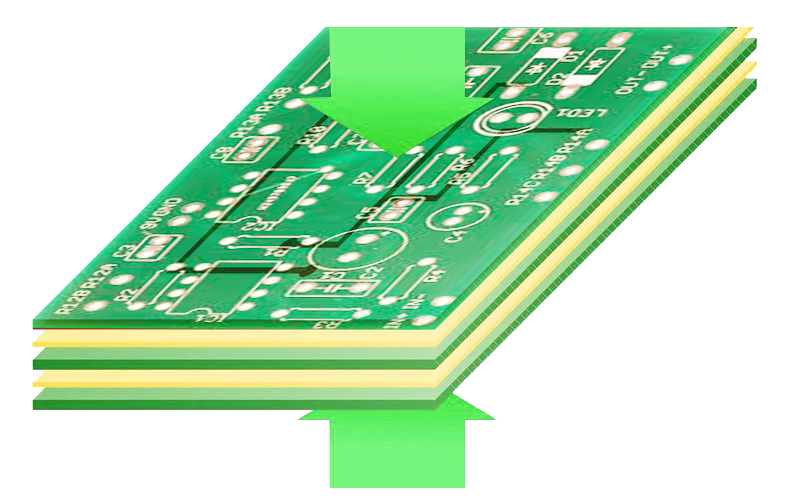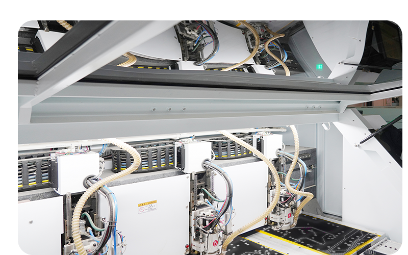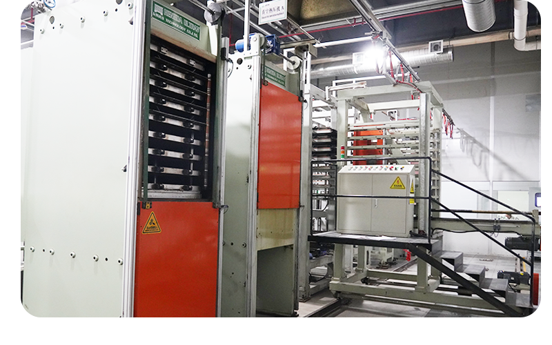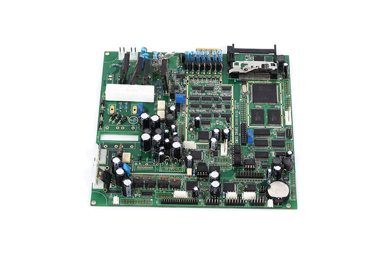

The PCB lamination process refers to the process of laminating each layer of circuit sheets of a multi-layer circuit board through a hot pressing process and laminating the PCB board with covering materials such as LCD screens and touch screens to firmly bond them together.
PCB lamination needs to be carried out under high temperature and pressure, so that the adhesive between the covering material and the PCB board can fully soften and flow, squeeze out the bubbles between the interfaces, and achieve high-strength bonding. The correct lamination process not only ensures the appearance but is also related to the reliability and service life of the product.
Lamination is an important process in the PCB manufacturing process. The main purposes of lamination are:
- Protect PCB Board From The External Environment
Lamination can form a protective layer on the PCB surface so that the PCB board is not directly exposed to the external environment. This can prevent the PCB from being damaged by mechanical collision, wear, corrosion, oxidation and other damage during transportation and use.
-Improve PCB Rigidity
Lamination can use materials such as fiberglass cloth to cover the PCB surface, thereby improving the mechanical strength and rigidity of the PCB. This is especially important for large-size PCBs.
- Isolate Conductive Paths
The lamination layer can play a role in isolating interconnection paths and preventing short circuits between different traces. This is especially important in high-density PCBs.
Therefore, lamination is an essential process in PCB production. Good lamination quality can ensure the functional performance and service life of the PCB.

PCB sheets need to be surface-treated before lamination to remove oil stains, oxide layers, etc. to ensure the adhesion between the glue and the sheet.
Commonly used surface treatment methods are:
- Chemical treatment: Use strong alkali or strong acid solutions to remove oil stains and oxide layers.
- Physical treatment: Using mechanical methods such as grinding wheels to remove burrs can also have a certain degree of decontamination at the same time.
- Gas treatment: Bombardment with high-pressure gases such as oxygen can achieve a certain decontamination effect.
The surface-treated PCB board needs to be strictly cleaned to ensure the smooth progress of subsequent processes.
An oxide layer is formed on the inner copper surface through chemical treatment, and the copper surface is roughened to increase adhesion. This process is called browning, which includes: opening semi-cured sheets, browning boards, and opening copper foils. What needs to be paid attention to in this process is the choice of glue. The choice of glue directly affects the lamination effect.
Commonly used pressure glues include:
- Epoxy glue: Fast curing speed, high bonding strength, and good heat resistance.
- Polyurethane glue: has excellent thermal shock resistance.
- Acrylic glue: high bonding strength and good solvent resistance.
Glue coating methods include scraping, screen printing, spraying, etc. After coating, the glue film thickness needs to be further controlled to avoid uneven lamination.
- Temperature: affects the bonding speed of glue, generally set at 100-180°C.
- Pressure: determines the thickness of the glue layer. If it is too low, it will result in insufficient pressure.
- Time: related to temperature and pressure, the glue is fully cured and should not be too long.
The best parameters need to be selected based on factors such as glue characteristics, plate type, thickness, etc.
According to the requirements of the manufacturing work order, subsequent processing such as shaping and edge grinding is carried out on the plates. Cut the pressed sheets into individual PCBs.

The quality of lamination directly affects the quality and service life of the PCB board. To achieve high-quality PCB lamination, the following aspects need to be strictly controlled:
Appearance inspection is the simplest and most intuitive inspection method. Mainly check whether there are obvious defects such as bubbles, degumming, and debris between the copper foil layer and the base material. These defects will affect the reliability of the printed circuit board.
During operation, check carefully from multiple angles under strong light and rework if any problems are found. Only when the appearance is good can subsequent electrical tests be carried out.
Resistance testing can detect whether there is a break in the press fit. The method is to pass a small current through both ends of the PCB and measure the resistance with a meter. If the resistance value is normal, it means the lamination is good; otherwise, there is a disconnection problem.
When conducting a resistance test, it should be noted that the contact resistance of the test lead will also bring into the test results, and the lead resistance is required to be as small as possible. The test should cover all copper foil channels on the PCB.
This is a key test to detect the tightness of the press fit. The method is to use a tensile tester to peel off part of the copper foil on the PCB and record the required peeling force value. If the peeling force is too small, it means insufficient lamination; if it is too large and difficult to peel off, it means excessive lamination.
The reasonable range of peel strength should be determined in advance by referring to the PCB design requirements. During the test, the peeling test should be carried out one by one, such as the four corners, straight edges, etc., to ensure that each area is pressed evenly

Problem: Uneven density or shape in the material indicates insufficient lamination.
Solution:
- Not Enough Glue Applied
If the glue is not evenly applied or the amount is insufficient, the PCB boards will not be well bonded together. When applying glue, ensure that the coverage area is sufficient and the coating thickness is moderate.
- Lamination Temperature Is Too Low
The laminating process needs to be carried out at a certain temperature. If the temperature is too low and the glue is not viscous enough, the PCB laminating effect will be poor. The general laminating temperature is 100-150°C.
- Insufficient Pressing Pressure
The applied pressure directly affects the bonding strength between PCB boards. If the pressure is insufficient, the contact between PCB boards is not tight, and the glue cannot penetrate well between the boards, resulting in poor lamination effect.
- Pressing Time is Too Short
Pressing takes a certain amount of time to allow the glue to fully penetrate between the PCB boards. If the pressing time is too short, the glue cannot be fully cured and the bonding strength between PCB boards will not be high. Generally, the pressing time needs to be guaranteed to be 30-90 minutes.
Problem: During the lamination process, air bubbles can become trapped in the material.
Solution: Make sure the raw materials are clean and dry to reduce bubble formation. Optimize press pressure and temperature settings to reduce air bubbles. Use a vacuum extraction system to remove air bubbles.
Problem: Choosing inappropriate materials can lead to product quality issues.
Solution: Carefully select materials that match the product requirements and consider the hardness, elasticity, thermal stability and other characteristics of the material.
Common PCB Lamination Covering Materials Are
- Transparent LCD display - can protect the PCB while allowing the display content to be seen
- Touch screen - Increase the interaction method of the product
- Transparent film - protective and aesthetic effect
- Metal cover - improve the thermal insulation and shielding effect of the product
上一条:PCB Drilling Explained: Dos and Don'ts and Best Capacities
